Nanotechnology manipulates matter at the atomic and molecular scale, typically below 100 nanometers, enabling innovations in medicine, electronics, and materials science. Microtechnology operates at micron-level dimensions, focusing on microscale devices like microelectromechanical systems (MEMS) used in sensors and actuators. Explore the distinctions and applications of these transformative technologies to understand their impact on modern science and engineering.
Main Difference
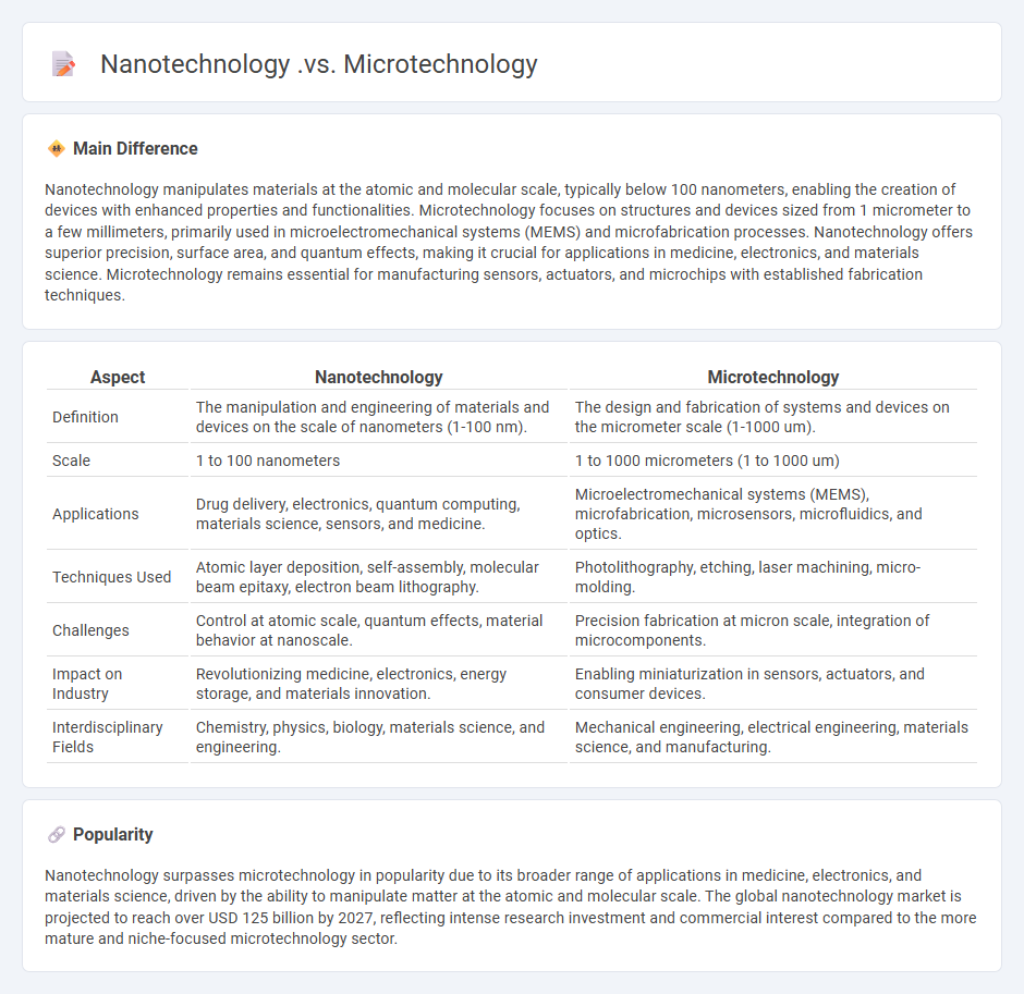
Nanotechnology manipulates materials at the atomic and molecular scale, typically below 100 nanometers, enabling the creation of devices with enhanced properties and functionalities. Microtechnology focuses on structures and devices sized from 1 micrometer to a few millimeters, primarily used in microelectromechanical systems (MEMS) and microfabrication processes. Nanotechnology offers superior precision, surface area, and quantum effects, making it crucial for applications in medicine, electronics, and materials science. Microtechnology remains essential for manufacturing sensors, actuators, and microchips with established fabrication techniques.
Connection
Nanotechnology and microtechnology intersect in the manipulation and fabrication of materials at increasingly smaller scales, with nanotechnology focusing on structures below 100 nanometers and microtechnology operating at the micrometer scale. Both fields drive advancements in electronics, medicine, and manufacturing by enabling precise control of material properties and device functionalities. Innovations such as micro-electromechanical systems (MEMS) often integrate nanoscale components, highlighting the synergy between these disciplines.
Comparison Table
| Aspect | Nanotechnology | Microtechnology |
|---|---|---|
| Definition | The manipulation and engineering of materials and devices on the scale of nanometers (1-100 nm). | The design and fabrication of systems and devices on the micrometer scale (1-1000 um). |
| Scale | 1 to 100 nanometers | 1 to 1000 micrometers (1 to 1000 um) |
| Applications | Drug delivery, electronics, quantum computing, materials science, sensors, and medicine. | Microelectromechanical systems (MEMS), microfabrication, microsensors, microfluidics, and optics. |
| Techniques Used | Atomic layer deposition, self-assembly, molecular beam epitaxy, electron beam lithography. | Photolithography, etching, laser machining, micro-molding. |
| Challenges | Control at atomic scale, quantum effects, material behavior at nanoscale. | Precision fabrication at micron scale, integration of microcomponents. |
| Impact on Industry | Revolutionizing medicine, electronics, energy storage, and materials innovation. | Enabling miniaturization in sensors, actuators, and consumer devices. |
| Interdisciplinary Fields | Chemistry, physics, biology, materials science, and engineering. | Mechanical engineering, electrical engineering, materials science, and manufacturing. |
Scale (Nanometer vs Micrometer)
Nanometers (nm) measure at the atomic and molecular scale, typically used to describe wavelengths of light, sizes of viruses, and dimensions of semiconductor components in nanotechnology. Micrometers (um) are one thousand times larger, commonly employed in biology for cell measurements, such as bacteria size around 1-10 um, and in engineering for precision manufacturing tolerances. Understanding the scale difference is crucial: 1 micrometer equals 1,000 nanometers, bridging the gap between nanoscale phenomena and larger microscopic structures. This distinction impacts scientific fields ranging from materials science to microbiology and electronics.
Manufacturing Techniques (Top-down vs Bottom-up)
Top-down manufacturing techniques involve starting with a bulk material and selectively removing parts to achieve the desired structure, commonly used in semiconductor fabrication and machining processes. Bottom-up manufacturing assembles products atom-by-atom or molecule-by-molecule, leveraging chemical synthesis and self-assembly methods prevalent in nanotechnology and 3D printing. Top-down methods often provide high precision for micro-scale features but can lead to material waste, while bottom-up approaches enable complex nanostructures with minimal waste and cost-effectiveness for small-scale production. Both techniques are integral to advanced manufacturing industries, including electronics, biomedical devices, and aerospace engineering.
Device Functionality (Quantum Effects vs Bulk Properties)
Quantum effects dominate device functionality when dimensions approach the nanoscale, enabling phenomena like tunneling, quantization, and discrete energy levels that bulk materials do not exhibit. Bulk properties arise from the collective behavior of large numbers of atoms, leading to classical electrical conductivity, thermal properties, and mechanical strength typically observed in macroscopic devices. Devices leveraging quantum effects, such as quantum dots, single-electron transistors, and quantum wells, exhibit enhanced sensitivity and novel functionalities absent in bulk-based counterparts. Understanding the interplay between quantum confinement and bulk behavior is critical for designing advanced nanoelectronic and optoelectronic devices.
Material Properties (Surface Area-to-Volume Ratio)
Materials with a high surface area-to-volume ratio exhibit enhanced chemical reactivity and faster heat transfer due to the larger exposed surface relative to their volume. Nanomaterials such as nanoparticles typically have ratios exceeding 60 m2/g, enabling applications in catalysis, drug delivery, and sensors. This property significantly influences processes such as diffusion, adsorption, and dissolution rates. Engineers often optimize this ratio to improve efficiency in systems involving mass and energy exchange.
Application Fields (Medicine, Electronics, Energy, MEMS, Drug Delivery)
Advancements in medicine leverage microscale technologies for precise diagnostics and targeted drug delivery systems, improving therapeutic outcomes. In electronics, microelectromechanical systems (MEMS) enhance sensor accuracy and device miniaturization, driving innovation in consumer and industrial applications. Energy applications utilize MEMS for efficient energy harvesting and storage, optimizing power management in compact devices. Drug delivery platforms integrate MEMS to enable controlled release mechanisms, enhancing treatment efficacy and patient compliance.
Source and External Links
### Set 1History of Microtechnologies and Nanotechnologies - This webpage provides definitions and historical context for both microtechnology and nanotechnology, highlighting their applications and differences in scale.
### Set 2About Microtechnology - This webpage explains microtechnology as the science of creating and controlling structures on a micrometer scale, often used in combination with nanotechnology for advanced applications.
### Set 3Nanotechnology and Microtechnology in Drug Delivery Systems - This article highlights the role of nanotechnology and microtechnology in improving drug delivery systems by enhancing therapeutic responses and patient compliance.
FAQs
What defines nanotechnology?
Nanotechnology is defined as the manipulation and control of matter at the atomic and molecular scale, typically between 1 and 100 nanometers.
What defines microtechnology?
Microtechnology is defined by the design, fabrication, and application of devices and systems with features typically ranging from 1 to 100 micrometers in size.
How do nanotechnology and microtechnology differ in scale?
Nanotechnology operates at the scale of 1 to 100 nanometers, whereas microtechnology functions at the micrometer scale, typically from 1 to 1000 micrometers.
What are the main applications of nanotechnology?
Nanotechnology is primarily applied in medicine for targeted drug delivery, electronics for miniaturized devices, energy for improved batteries and solar cells, materials science for stronger and lighter materials, and environmental science for pollution control and water purification.
What are the main applications of microtechnology?
Microtechnology is primarily applied in electronics manufacturing, medical devices, microelectromechanical systems (MEMS), telecommunications, and precision instrumentation.
What materials are commonly used in each technology?
3D printing commonly uses PLA, ABS, resin, nylon, and metal powders; CNC machining frequently utilizes aluminum, steel, brass, and plastics; injection molding primarily employs thermoplastics like polypropylene, polyethylene, and polystyrene; and laser cutting often cuts materials such as acrylic, wood, fabric, and metal sheets.
How do nanotechnology and microtechnology impact modern electronics?
Nanotechnology and microtechnology enhance modern electronics by enabling smaller, faster, and more energy-efficient devices with improved performance and novel functionalities such as flexible electronics and advanced sensors.