Nanophotonics explores the behavior of light on the nanometer scale, focusing on manipulating photons through materials and structures smaller than the wavelength of light. Plasmonics investigates the interaction between electromagnetic waves and free electrons in metals, enabling subwavelength light confinement and enhanced optical fields. Discover more about how these fields converge to revolutionize sensing, imaging, and communication technologies.
Main Difference
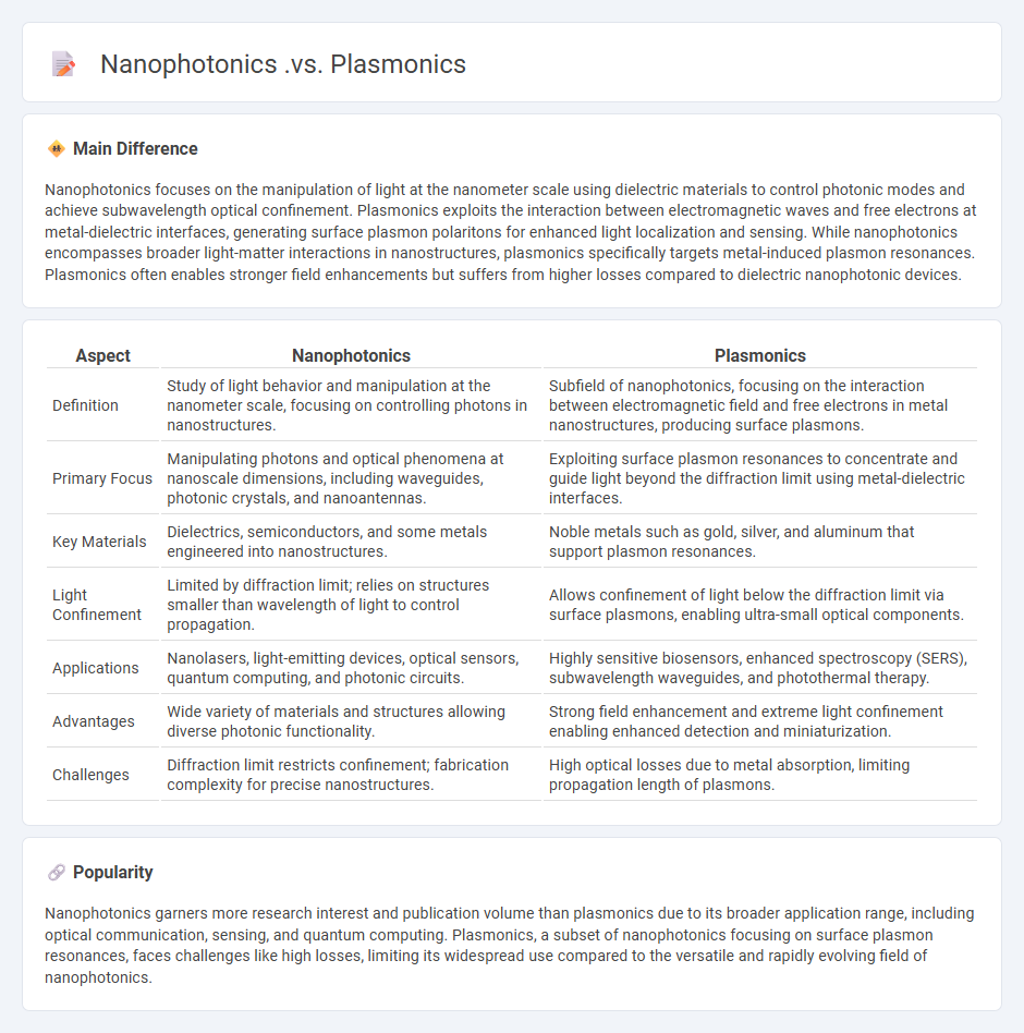
Nanophotonics focuses on the manipulation of light at the nanometer scale using dielectric materials to control photonic modes and achieve subwavelength optical confinement. Plasmonics exploits the interaction between electromagnetic waves and free electrons at metal-dielectric interfaces, generating surface plasmon polaritons for enhanced light localization and sensing. While nanophotonics encompasses broader light-matter interactions in nanostructures, plasmonics specifically targets metal-induced plasmon resonances. Plasmonics often enables stronger field enhancements but suffers from higher losses compared to dielectric nanophotonic devices.
Connection
Nanophotonics and plasmonics are interconnected fields that manipulate light at the nanoscale, enhancing optical phenomena beyond the diffraction limit. Plasmonics focuses on surface plasmons, which are collective oscillations of electrons at metal-dielectric interfaces, enabling strong light confinement and field enhancement. These effects in plasmonics are foundational to many nanophotonic applications, including sensing, imaging, and information processing at subwavelength scales.
Comparison Table
| Aspect | Nanophotonics | Plasmonics |
|---|---|---|
| Definition | Study of light behavior and manipulation at the nanometer scale, focusing on controlling photons in nanostructures. | Subfield of nanophotonics, focusing on the interaction between electromagnetic field and free electrons in metal nanostructures, producing surface plasmons. |
| Primary Focus | Manipulating photons and optical phenomena at nanoscale dimensions, including waveguides, photonic crystals, and nanoantennas. | Exploiting surface plasmon resonances to concentrate and guide light beyond the diffraction limit using metal-dielectric interfaces. |
| Key Materials | Dielectrics, semiconductors, and some metals engineered into nanostructures. | Noble metals such as gold, silver, and aluminum that support plasmon resonances. |
| Light Confinement | Limited by diffraction limit; relies on structures smaller than wavelength of light to control propagation. | Allows confinement of light below the diffraction limit via surface plasmons, enabling ultra-small optical components. |
| Applications | Nanolasers, light-emitting devices, optical sensors, quantum computing, and photonic circuits. | Highly sensitive biosensors, enhanced spectroscopy (SERS), subwavelength waveguides, and photothermal therapy. |
| Advantages | Wide variety of materials and structures allowing diverse photonic functionality. | Strong field enhancement and extreme light confinement enabling enhanced detection and miniaturization. |
| Challenges | Diffraction limit restricts confinement; fabrication complexity for precise nanostructures. | High optical losses due to metal absorption, limiting propagation length of plasmons. |
Light Manipulation at Nanoscale
Light manipulation at the nanoscale involves controlling electromagnetic waves using nanostructures smaller than the wavelength of visible light, typically below 100 nanometers. Techniques such as plasmonics exploit the resonant oscillation of free electrons in metallic nanoparticles to concentrate and guide light at subwavelength scales. Nanophotonic devices, including metasurfaces and photonic crystals, enable unprecedented control over light properties like phase, amplitude, and polarization for applications in sensing, imaging, and information processing. Advances in materials like graphene and transition metal dichalcogenides further enhance the efficiency and tunability of nanoscale light manipulation technologies.
Surface Plasmon Resonance (SPR)
Surface Plasmon Resonance (SPR) is an advanced optical detection technique widely used for analyzing biomolecular interactions in real time without labeling. It measures changes in refractive index near the sensor surface when biomolecules bind, providing precise kinetic data such as association and dissociation rates. SPR systems employ gold-coated sensor chips and polarized light to generate surface plasmons, enabling sensitive detection at picomolar concentrations. This technology is critical in drug discovery, antibody characterization, and studying protein-protein, protein-DNA, and small molecule interactions.
Subwavelength Confinement
Subwavelength confinement refers to the ability to confine electromagnetic waves to dimensions smaller than their wavelength, enabling enhanced light-matter interaction. This phenomenon is critical in nanophotonics and plasmonics, where structures such as photonic crystals and metal nanoparticles manipulate light at the nanoscale. Applications include super-resolution imaging, highly sensitive sensors, and efficient light sources for integrated photonic circuits. Advances in materials like graphene and metamaterials have further pushed the limits of subwavelength confinement efficiency and control.
Photonic Crystals vs Metal Nanostructures
Photonic crystals manipulate light through periodic dielectric structures, creating photonic band gaps that control photon propagation with high precision. Metal nanostructures, such as plasmonic nanoparticles, exploit localized surface plasmon resonances to concentrate electromagnetic fields at the nanoscale, enhancing light-matter interactions. Photonic crystals typically excel in low-loss optical applications like waveguides and optical filters, whereas metal nanostructures are crucial in sensing, surface-enhanced Raman scattering (SERS), and nanoantennas due to their strong field enhancement. Advances in integrated photonics increasingly combine both platforms to achieve tailored optical responses across visible and near-infrared spectra.
Optical Sensing and Information Processing
Optical sensing technologies utilize light-based mechanisms to detect and measure physical, chemical, and biological parameters with high precision. Advanced information processing algorithms enhance data analysis, enabling real-time interpretation and decision-making in applications such as environmental monitoring, medical diagnostics, and industrial automation. Innovations in photonic devices and integrated optical circuits improve sensitivity and speed while reducing energy consumption. These advancements support the development of intelligent systems that leverage optical signals for efficient and accurate information retrieval.
Source and External Links
Plasmonics and Nanophotonics - NanoComposix - Plasmonics is a subfield of nanophotonics focusing on metallic nanoparticles that manipulate light via surface plasmons, enabling strong absorption and scattering, while nanophotonics broadly deals with controlling electromagnetic fields at the nanoscale including plasmonics, photonic crystals, and metamaterials.
Plasmonics and nanophotonics - SDU - Nanophotonics encompasses the generation and control of electromagnetic fields at nanoscale and includes plasmonics, which explores electron oscillations in metals leading to unique optical properties; nanophotonics covers a wider range of phenomena including photonic crystals and metamaterials.
Lec 1: Introduction to Nanophotonics & Plasmonics - YouTube - Plasmonics, a subfield of nanophotonics, studies surface plasmon oscillations in metallic nanostructures enabling confinement of electromagnetic fields below the diffraction limit, facilitating nanoscale photonic devices, while nanophotonics is the broader field involving manipulation of light at the nanoscale across materials and structures.
FAQs
What is nanophotonics?
Nanophotonics is the study and manipulation of light on the nanometer scale, focusing on interactions between photons and nanostructured materials to develop advanced optical devices.
What is plasmonics?
Plasmonics is the study and application of surface plasmons--coherent electron oscillations at the interface between a metal and a dielectric--that enable subwavelength light manipulation and enhanced electromagnetic field confinement.
How do nanophotonics and plasmonics differ?
Nanophotonics studies light behavior and manipulation at the nanometer scale, focusing on dielectric and semiconductor nanostructures, while plasmonics specifically investigates surface plasmon resonances in metal nanostructures to confine and control light beyond the diffraction limit.
What materials are used in nanophotonics and plasmonics?
Common materials used in nanophotonics and plasmonics include noble metals like gold (Au) and silver (Ag) for their strong plasmonic properties, semiconductors such as silicon (Si) and gallium arsenide (GaAs) for optical functionality, and dielectric materials like silicon dioxide (SiO2) and titanium dioxide (TiO2) for waveguiding and light manipulation.
What are the main applications of nanophotonics?
Nanophotonics is primarily applied in optical communication, high-resolution imaging, sensing, data storage, and photonic computing.
What are the main applications of plasmonics?
Plasmonics is primarily applied in biosensing, photothermal therapy, enhancing solar cell efficiency, improving optical communication, and developing nanoscale photonic devices.
How do nanophotonic and plasmonic devices influence future technologies?
Nanophotonic and plasmonic devices enhance future technologies by enabling ultra-compact optical circuits, improving data transmission speeds with reduced energy consumption, and advancing high-resolution sensing and imaging systems.