Photolithography and Electron Beam Lithography (EBL) are essential techniques in semiconductor manufacturing, each offering unique advantages in pattern resolution and processing speed. Photolithography excels in high-throughput mass production with feature sizes typically around 7 nm to 193 nm, utilizing ultraviolet light to transfer patterns onto wafers. Electron Beam Lithography provides unparalleled precision for nanoscale features below 10 nm by directly writing with a focused electron beam, making it crucial for research and prototyping. Explore further to understand which lithography method suits your application needs best.
Main Difference
Photolithography uses ultraviolet light to transfer geometric patterns from a photomask onto a photoresist-coated substrate, enabling high-throughput semiconductor fabrication with feature sizes typically above 20 nm. Electron Beam Lithography (EBL) employs a focused electron beam to directly write patterns onto the resist, achieving much finer resolutions below 10 nm but at slower speeds and higher costs. Photolithography is ideal for mass production in integrated circuits due to its rapid processing, while EBL is preferred for research, prototyping, and mask-making because of its precision. Both techniques play crucial roles in nanofabrication, with complementary strengths in scalability and resolution.
Connection
Photolithography and electron beam lithography (EBL) are both critical techniques used in semiconductor manufacturing to pattern micro- and nanoscale features on substrates. Photolithography employs ultraviolet light and masks to transfer patterns quickly over large areas, whereas EBL utilizes a focused electron beam to directly write high-resolution patterns without masks, enabling finer detail at the expense of slower throughput. These methods are often combined in fabrication processes, with photolithography handling broader structures and EBL refining intricate nanoscale features for advanced device architectures.
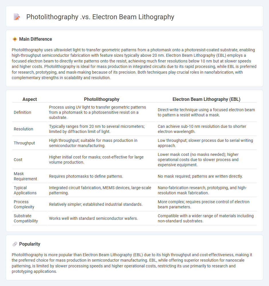
Comparison Table
| Aspect | Photolithography | Electron Beam Lithography (EBL) |
|---|---|---|
| Definition | Process using UV light to transfer geometric patterns from a photomask to a photosensitive resist on a substrate. | Direct-write technique using a focused electron beam to pattern a resist without a mask. |
| Resolution | Typically ranges from 20 nm to several micrometers; limited by diffraction limit of light. | Can achieve sub-10 nm resolution due to shorter electron wavelength. |
| Throughput | High throughput; suitable for mass production in semiconductor manufacturing. | Low throughput; slower process due to serial writing approach. |
| Cost | Higher initial cost for masks; cost-effective for large volume production. | Lower mask cost (no masks needed); higher operational costs due to slower process and expensive equipment. |
| Mask Requirement | Requires photomasks to define patterns. | No mask required; patterns are written directly. |
| Typical Applications | Integrated circuit fabrication, MEMS devices, large-scale patterning. | Nano-fabrication research, prototyping, and high-resolution mask fabrication. |
| Process Complexity | Relatively simpler; established industrial standards. | More complex; requires precise control of electron beam parameters. |
| Substrate Compatibility | Works well with standard semiconductor wafers. | Compatible with a wider range of materials including non-standard substrates. |
Resolution
Resolution in engineering refers to the smallest measurable increment or detail that a system or instrument can detect or display. High-resolution measurement devices, such as digital calipers or laser scanners, enable precise detection of minute differences in dimensions or signals. In fields like computer graphics and instrumentation, higher resolution translates into greater accuracy and finer detail representation. Resolution impacts performance, accuracy, and reliability across engineering applications including CAD modeling, control systems, and quality inspection.
Throughput
Throughput in engineering measures the rate at which a system processes inputs into outputs, often expressed in units per second or transactions per hour. It directly impacts manufacturing efficiency, network data transfer, and production capacity in various engineering fields. Improving throughput involves optimizing system components, reducing bottlenecks, and enhancing process flow to maximize operational productivity. High throughput correlates with reduced cycle times and increased resource utilization.
Mask Requirement
Mask requirements in engineering projects focus on ensuring worker safety by minimizing exposure to hazardous airborne particles such as dust, chemicals, and gases. Industry standards like OSHA mandate specific types of respiratory protection based on the nature of contaminants and workplace conditions. Certified masks, including N95 respirators or half-face respirators, are commonly used in construction, manufacturing, and chemical processing. Proper mask selection and fit testing are critical to comply with safety regulations and prevent occupational illnesses.
Cost Efficiency
Cost efficiency in engineering involves optimizing resource utilization to minimize expenses while maximizing project output and quality. Implementing advanced technologies, such as automation and predictive maintenance, reduces operational costs and downtime. Strategic project management techniques streamline workflows and prevent budget overruns. Analyzing lifecycle costs ensures sustainable investment in materials, labor, and equipment throughout the engineering process.
Application Suitability
Application suitability in engineering refers to the evaluation of materials, processes, and technologies to ensure they meet specific project requirements such as durability, cost-efficiency, and environmental impact. Engineers assess factors like mechanical strength, thermal resistance, and compatibility with existing systems to determine the best solutions for construction, manufacturing, or software development. Advanced simulation tools and standards like ASTM or ISO guide this selection process to optimize performance and safety. Prioritizing application suitability reduces risk and enhances project sustainability and innovation.
Source and External Links
Electron-beam lithography - Electron-beam lithography uses a focused beam of electrons to create high-resolution patterns on a surface, often for low-volume production or research due to its slow throughput.
Electron Beam and Optical Lithography - This comparison highlights electron beam lithography's ability to achieve higher resolution than optical lithography, albeit with slower processing times.
Photolithography vs E Beam Lithography - Photolithography uses light and is faster, while electron beam lithography uses electrons for higher resolution but slower processing, making it more suitable for specialized applications.
FAQs
What is photolithography in microfabrication?
Photolithography in microfabrication is a process that uses light to transfer a geometric pattern from a photomask onto a photosensitive resist layer on a semiconductor wafer, enabling precise etching or material deposition for integrated circuit production.
What is electron beam lithography used for?
Electron beam lithography is used for creating extremely precise nanoscale patterns in semiconductor device fabrication and nanotechnology research.
How does photolithography work?
Photolithography uses light to transfer a geometric pattern from a photomask onto a light-sensitive photoresist layer on a semiconductor wafer, defining precise circuit features for microchip fabrication.
How does electron beam lithography differ from photolithography?
Electron beam lithography uses a focused electron beam to achieve nanometer-scale patterning with high resolution, while photolithography employs ultraviolet light through masks, limiting resolution due to diffraction effects.
What materials are used in each lithography technique?
Photolithography uses photoresist materials such as positive or negative photoresists; electron beam lithography employs electron-sensitive resists like PMMA; extreme ultraviolet lithography uses EUV photoresists based on chemically amplified resists; nanoimprint lithography relies on UV-curable polymers or thermoplastic materials; and X-ray lithography utilizes X-ray resists like PMMA or copolymers sensitive to X-rays.
What are the resolution limits of photolithography vs electron beam lithography?
Photolithography typically achieves resolution limits around 20-30 nanometers with advanced extreme ultraviolet (EUV) techniques, while electron beam lithography can reach resolutions below 10 nanometers, often 5 nm or less, due to its direct-write capability and shorter electron wavelength.
Why choose electron beam lithography over photolithography?
Electron beam lithography offers superior resolution below 10 nanometers, enabling patterning of extremely fine features essential for advanced semiconductor devices, unlike photolithography which is limited by light diffraction to larger feature sizes.