Spin coating produces uniform thin films rapidly by depositing a solution on a substrate and spinning it at high speeds, ideal for microelectronics and optics. Dip coating involves immersing and withdrawing a substrate from a solution, allowing precise control over film thickness and composition, commonly used in biomedical and corrosion-resistant coatings. Explore detailed comparisons to determine the best method for your specific application requirements.
Main Difference
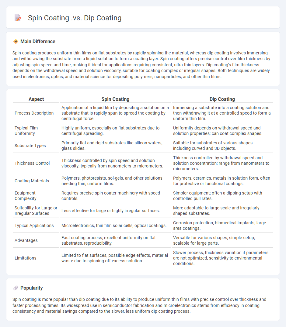
Spin coating produces uniform thin films on flat substrates by rapidly spinning the material, whereas dip coating involves immersing and withdrawing the substrate from a liquid solution to form a coating layer. Spin coating offers precise control over film thickness by adjusting spin speed and time, making it ideal for applications requiring consistent, ultra-thin layers. Dip coating's film thickness depends on the withdrawal speed and solution viscosity, suitable for coating complex or irregular shapes. Both techniques are widely used in electronics, optics, and material science for depositing polymers, nanoparticles, and other thin films.
Connection
Spin coating and dip coating are both thin film deposition techniques used to create uniform coatings on substrates in industries like electronics and optics. Spin coating uses centrifugal force to spread a liquid film evenly by rapidly spinning the substrate, while dip coating involves immersing and withdrawing the substrate from a coating solution at a controlled speed. Both methods rely on fluid dynamics and surface tension to achieve precise film thickness and uniformity for applications such as semiconductor fabrication and sensor production.
Comparison Table
| Aspect | Spin Coating | Dip Coating |
|---|---|---|
| Process Description | Application of a liquid film by depositing a solution on a substrate that is rapidly spun to spread the coating by centrifugal force. | Immersing a substrate into a coating solution and then withdrawing it at a controlled speed to form a uniform thin film. |
| Typical Film Uniformity | Highly uniform, especially on flat substrates due to centrifugal spreading. | Uniformity depends on withdrawal speed and solution properties; can coat complex shapes. |
| Substrate Types | Primarily flat and rigid substrates like silicon wafers, glass slides. | Suitable for substrates of various shapes including curved and 3D objects. |
| Thickness Control | Thickness controlled by spin speed and solution viscosity; typically from nanometers to micrometers. | Thickness controlled by withdrawal speed and solution concentration; range from nanometers to micrometers. |
| Coating Materials | Polymers, photoresists, sol-gels, and other solutions needing thin, uniform films. | Polymers, ceramics, metals in solution form, often for protective or functional coatings. |
| Equipment Complexity | Requires precise spin coater machinery with speed controls. | Simpler equipment; often a dipping setup with controlled pull rates. |
| Suitability for Large or Irregular Surfaces | Less effective for large or highly irregular surfaces. | More adaptable to large scale and irregularly shaped substrates. |
| Typical Applications | Microelectronics, thin film solar cells, optical coatings. | Corrosion protection, biomedical implants, large area coatings. |
| Advantages | Fast coating process, excellent uniformity on flat substrates, reproducibility. | Versatile for various shapes, simple setup, scalable for large parts. |
| Limitations | Limited to flat surfaces, possible edge effects, material waste due to spinning off excess solution. | Slower process, thickness variation if parameters are not optimized, sensitivity to environmental conditions. |
Thin Film Deposition
Thin film deposition is a critical process in engineering that involves the precise application of ultra-thin material layers onto substrates, enhancing the performance and functionality of electronic devices, optical coatings, and MEMS components. Techniques such as Physical Vapor Deposition (PVD), Chemical Vapor Deposition (CVD), and Atomic Layer Deposition (ALD) enable controlled thickness at the nanometer scale, essential for semiconductor manufacturing and advanced material engineering. Industrial applications include the production of integrated circuits, solar cells, and hard coatings for aerospace components, demonstrating significant improvements in durability and efficiency. Optimization of deposition parameters like temperature, pressure, and precursor flow rates directly affects film quality, uniformity, and adhesion, which are key to device reliability.
Coating Uniformity
Coating uniformity in engineering ensures consistent thickness and adhesion across surfaces, critical for product durability and performance. Advanced techniques like spray coating, dip coating, and spin coating optimize uniformity by controlling parameters such as viscosity, application speed, and environmental conditions. Precision measurement tools like laser profilometers and optical microscopy assess uniformity at micrometer scales, facilitating quality control in industries including aerospace, automotive, and electronics manufacturing. Uniform coatings prevent defects such as corrosion, wear, and electrical failures, significantly enhancing component lifespan and functionality.
Substrate Geometry
Substrate geometry significantly influences the mechanical performance and durability of engineering materials, particularly in electronic packaging and composite structures. Precise control of substrate thickness, shape, and surface topology optimizes stress distribution and thermal management. Finite element analysis (FEA) is commonly employed to model substrate geometry effects, enhancing design accuracy and reliability. Advanced substrates with tailored geometries improve structural integrity and facilitate miniaturization in microelectronics and aerospace applications.
Material Wastage
Material wastage in engineering significantly impacts project costs and environmental sustainability, accounting for up to 30% of total material expenses in construction and manufacturing sectors. Efficient resource management techniques, such as lean manufacturing and precise material estimation, can reduce wastage by 15-25%. Advanced technologies like 3D printing and computer-aided design (CAD) optimize material usage through accurate modeling and minimized offcuts. Implementing recycling and reuse strategies further decreases environmental footprint, promoting circular economy principles in engineering projects.
Industrial Applications
Industrial applications in engineering encompass the design, development, and implementation of machinery, systems, and processes that optimize production efficiency across sectors such as manufacturing, energy, and automotive industries. Advanced techniques like computer-aided design (CAD), automation, and robotics significantly improve precision and reduce operational costs. Integration of Internet of Things (IoT) sensors facilitates real-time monitoring and predictive maintenance, minimizing downtime in industrial plants. Emerging trends focus on sustainable engineering solutions to reduce environmental impact and enhance resource efficiency.
Source and External Links
Spin Coating vs. Dip Coating: Which One Is Right for Your Application? - Spin coating uses centrifugal force to create highly uniform, fast, and precisely controlled thin films ideal for microfabrication and optoelectronics, whereas dip coating is a simpler immersion process more suited for coating entire objects without such uniformity requirements.
The Ultimate Guide To Spin Coating Processes - Dip-spin coating combines dip and spin coating to coat complex 3D objects evenly by dipping followed by spinning to remove excess material, with more processing steps than regular spin coating.
Dip Coating vs. Spin Coating: When To Use Which Method - Dip coating involves immersion and curing and is straightforward for larger parts, whereas spin coating coats small parts by spinning off excess material; spin coating is limited by basket size and best for small hardware components.
FAQs
What is spin coating?
Spin coating is a technique used to apply uniform thin films onto flat substrates by depositing a liquid solution and spinning the substrate at high speeds to spread and thin the layer.
What is dip coating?
Dip coating is a manufacturing process where a substrate is immersed into a liquid coating solution and then withdrawn to form a uniform thin film as the liquid dries or cures.
What are the main differences between spin coating and dip coating?
Spin coating uses centrifugal force to spread a liquid film uniformly on a substrate by rapid rotation, resulting in thin, even coatings ideal for microelectronics, while dip coating involves immersing and withdrawing a substrate from a solution, producing thicker, more uniform coatings suitable for large surfaces and industrial applications.
What materials can be used with spin coating?
Spin coating can be used with materials such as photoresists, polymers, sol-gels, nanoparticles, and thin film precursors for electronics and optics applications.
What are the advantages of dip coating?
Dip coating offers advantages such as uniform film thickness, excellent surface coverage, cost-effectiveness, scalability for large or complex shapes, and compatibility with various materials and substrates.
How does thickness control differ in spin coating and dip coating?
In spin coating, thickness is mainly controlled by spin speed, spin time, and solution viscosity; higher spin speeds and lower viscosities yield thinner films. In dip coating, film thickness depends primarily on withdrawal speed, solution concentration, and fluid viscosity; faster withdrawal speeds and higher viscosities produce thicker coatings.
Which applications require spin coating or dip coating?
Spin coating or dip coating is required in applications such as semiconductor wafer fabrication, thin film deposition for solar cells, optical coatings, biomedical device manufacturing, and protective or functional coatings on glass and polymers.