Photonic crystals manipulate light through periodic dielectric structures, enabling precise control over electromagnetic wave propagation and photonic band gaps. Metamaterials consist of engineered subwavelength structures designed to achieve unconventional electromagnetic properties not found in natural materials, such as negative refractive index. Explore the unique characteristics and applications of photonic crystals and metamaterials to understand their impact on modern optics and nanotechnology.
Main Difference
Photonic crystals are periodic optical nanostructures that affect the motion of photons by creating photonic band gaps, preventing light of certain wavelengths from propagating through the material. Metamaterials are artificially engineered composites designed to have electromagnetic properties not found in natural materials, often manipulating wave propagation through subwavelength structuring. Photonic crystals rely on Bragg scattering and periodicity to control light, while metamaterials exploit resonant structures to achieve negative refractive indices or cloaking effects. The key distinction lies in photonic crystals' wavelength-scale periodicity versus metamaterials' subwavelength unit cells tailored for exotic electromagnetic responses.
Connection
Photonic crystals and metamaterials both manipulate electromagnetic waves through engineered periodic structures, enabling control over light propagation at subwavelength scales. Photonic crystals achieve bandgap effects by creating periodic dielectric contrasts, while metamaterials derive unique optical properties from artificially structured unit cells with tailored electromagnetic responses. Their interconnection lies in the design principles that exploit periodicity and resonance phenomena to achieve novel functionalities in optics and photonics.
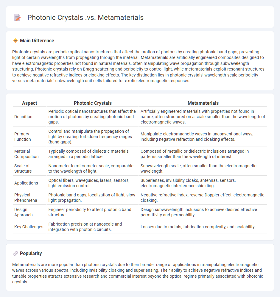
Comparison Table
| Aspect | Photonic Crystals | Metamaterials |
|---|---|---|
| Definition | Periodic optical nanostructures that affect the motion of photons by creating photonic band gaps. | Artificially engineered materials with properties not found in nature, often structured on a scale smaller than the wavelength of electromagnetic waves. |
| Primary Function | Control and manipulate the propagation of light by creating forbidden frequency ranges (band gaps). | Manipulate electromagnetic waves in unconventional ways, including negative refraction and cloaking effects. |
| Material Composition | Typically composed of dielectric materials arranged in a periodic lattice. | Composed of metallic or dielectric inclusions arranged in patterns smaller than the wavelength of interest. |
| Scale of Structure | Nanometer to micrometer scale, comparable to the wavelength of light. | Subwavelength scale, often smaller than the electromagnetic wavelength. |
| Applications | Optical fibers, waveguides, lasers, sensors, light emission control. | Superlenses, invisibility cloaks, antennas, sensors, electromagnetic interference shielding. |
| Physical Phenomena | Photonic band gaps, localization of light, slow light propagation. | Negative refractive index, reverse Doppler effect, electromagnetic cloaking. |
| Design Approach | Engineer periodicity to affect photonic band structure. | Design subwavelength inclusions to achieve desired effective permittivity and permeability. |
| Key Challenges | Fabrication precision at nanoscale and integration with photonic circuits. | Losses due to metals, fabrication complexity, and scalability. |
Bandgap Engineering
Bandgap engineering involves the deliberate manipulation of the electronic band structure of semiconductor materials to tailor their electrical and optical properties. Techniques such as alloying, quantum well formation, and strain application enable precise control over bandgap energy, which is critical for optimizing device performance in applications like photovoltaics, light-emitting diodes, and high-speed transistors. Materials like gallium arsenide (GaAs) and indium gallium nitride (InGaN) are commonly used due to their tunable bandgaps ranging from 0.7 eV to over 3.4 eV. Advances in molecular beam epitaxy (MBE) and metal-organic chemical vapor deposition (MOCVD) facilitate atomic-scale bandgap modifications for next-generation optoelectronic devices.
Refractive Index Manipulation
Refractive index manipulation is a critical technique in engineering, enabling the control of light propagation within various materials to enhance optical device performance. Advanced methods such as photonic crystal design and metamaterials allow precise tuning of the refractive index, facilitating applications in fiber optics, lens fabrication, and sensor technology. Engineers exploit these variations to create components like waveguides, optical filters, and cloaking devices that improve signal clarity and reduce loss. Cutting-edge research in nano-engineering further expands the potential for refractive index engineering in telecommunications and imaging systems.
Electromagnetic Wave Control
Electromagnetic wave control involves manipulating the propagation, reflection, absorption, and transmission properties of electromagnetic waves to optimize performance in engineering applications. Techniques such as metamaterials, phased array antennas, and tunable filters enable precise control over wave behavior across the spectrum from radio frequencies to terahertz and optical ranges. Advanced electromagnetic wave control enhances wireless communication systems, radar technology, and medical imaging by improving signal clarity, reducing interference, and enabling dynamic beam steering. Research in this field integrates material science, computational electromagnetics, and nanotechnology to develop innovative solutions for efficient energy management and data transmission.
Structural Periodicity
Structural periodicity in engineering refers to the repetitive arrangement of elements or components within a structure, enhancing mechanical properties and stability. Common examples include truss bridges, lattice frameworks, and modular building systems, which utilize repeating units to distribute loads efficiently and reduce material use. The periodic pattern influences vibration modes, wave propagation, and stress distribution, critical factors in the design of aerospace, civil, and mechanical engineering structures. Advanced computational models often simulate periodicity effects to optimize durability and performance under dynamic conditions.
Tunable Optical Properties
Tunable optical properties enable precise control of light-matter interactions in engineering applications, enhancing the performance of photonic devices such as lasers, sensors, and optical switches. Materials like graphene, liquid crystals, and metamaterials exhibit adjustable refractive indices, absorption rates, and emission spectra under external stimuli including electric fields, temperature changes, and mechanical strain. Advances in nanofabrication techniques facilitate the integration of these tunable materials into compact, efficient systems used in telecommunications, medical imaging, and environmental monitoring. Optimization of these properties improves device sensitivity, speed, and energy efficiency across various engineering disciplines.
Source and External Links
Photonic Crystals as Metamaterials - Discusses why some photonic crystals show metamaterial properties, often due to their optical band gaps.
Photonic Meta-Crystals - Introduces the concept of photonic meta-crystals, which integrate photonic crystals and metamaterials to enhance light-matter interactions.
Photonic Metamaterial - Explores photonic metamaterials, which are distinguished from photonic crystals by their subwavelength periodicity and interaction with light across various wavelengths.
FAQs
What are photonic crystals?
Photonic crystals are materials with a periodic structure that affects the motion of photons, creating photonic band gaps that control the propagation of light.
What are metamaterials?
Metamaterials are artificially engineered materials designed to have unique electromagnetic properties not found in natural materials, enabling control over waves such as light and sound.
How do photonic crystals differ from metamaterials?
Photonic crystals differ from metamaterials by possessing a periodically structured dielectric medium that affects light propagation via photonic bandgaps, whereas metamaterials are artificially engineered composites with subwavelength inclusions designed to achieve unusual electromagnetic properties not found in natural materials.
What are photonic crystals made of?
Photonic crystals are made of periodic dielectric materials with contrasting refractive indices, such as silicon, gallium arsenide, or polymer composites.
What is the main function of metamaterials?
Metamaterials primarily function to manipulate electromagnetic waves in unconventional ways, enabling control over properties such as refraction, absorption, and scattering.
How do photonic crystals control light?
Photonic crystals control light by creating periodic dielectric structures that produce photonic band gaps, preventing specific light wavelengths from propagating and enabling precise manipulation of light flow.
Where are photonic crystals and metamaterials used?
Photonic crystals and metamaterials are used in optical fibers, sensors, lasers, cloaking devices, antennas, and imaging systems.