Chemical Vapor Deposition (CVD) and Physical Vapor Deposition (PVD) are prominent thin film coating techniques utilized in electronics, optics, and materials engineering, each offering unique advantages in terms of film quality, adhesion, and uniformity. CVD involves chemical reactions to produce a solid material on a substrate, creating excellent coverage and conformality, while PVD relies on physical processes like evaporation or sputtering, enabling precise control of film thickness and composition. Explore the critical differences and applications of CVD and PVD to determine the ideal method for your advanced surface coating needs.
Main Difference
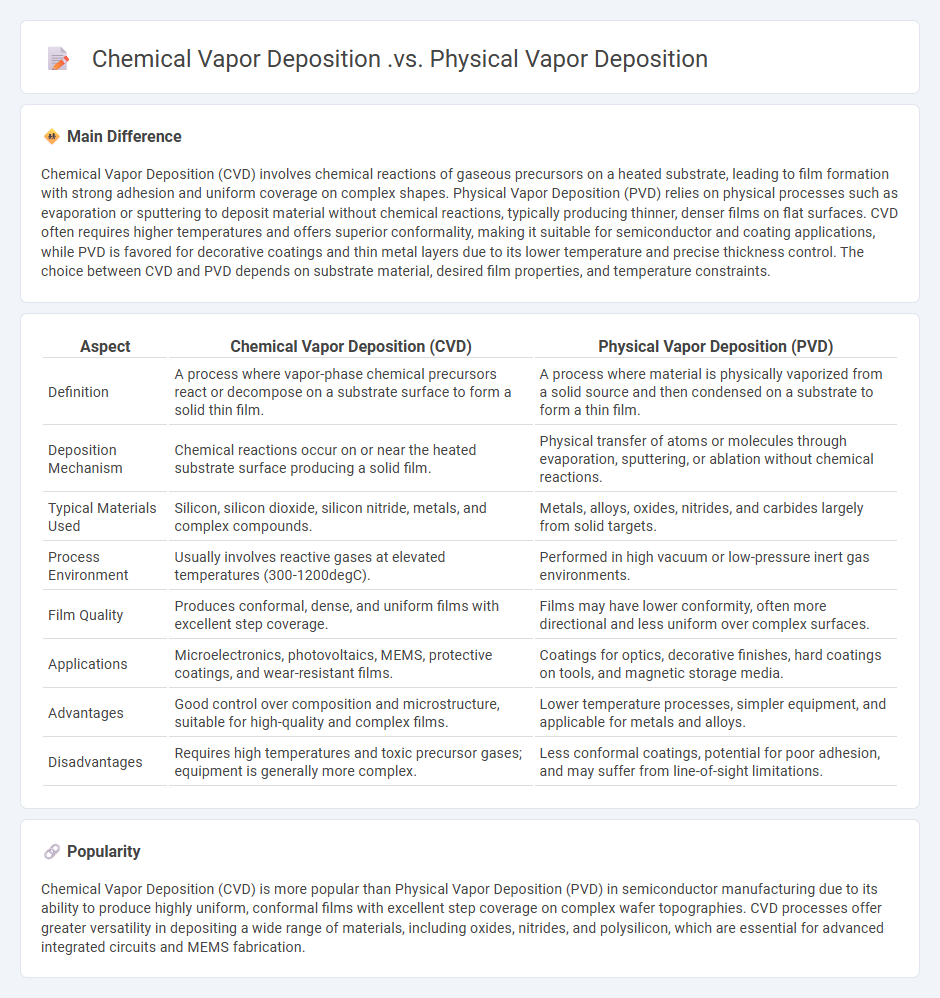
Chemical Vapor Deposition (CVD) involves chemical reactions of gaseous precursors on a heated substrate, leading to film formation with strong adhesion and uniform coverage on complex shapes. Physical Vapor Deposition (PVD) relies on physical processes such as evaporation or sputtering to deposit material without chemical reactions, typically producing thinner, denser films on flat surfaces. CVD often requires higher temperatures and offers superior conformality, making it suitable for semiconductor and coating applications, while PVD is favored for decorative coatings and thin metal layers due to its lower temperature and precise thickness control. The choice between CVD and PVD depends on substrate material, desired film properties, and temperature constraints.
Connection
Chemical Vapor Deposition (CVD) and Physical Vapor Deposition (PVD) are complementary thin film deposition techniques used in semiconductor manufacturing and surface engineering. Both processes involve the formation of solid materials on substrates by vapor phase methods, but CVD relies on chemical reactions of gaseous precursors while PVD depends on physical processes like sputtering or evaporation. These methods are often integrated in advanced fabrication workflows to achieve precise control over film composition, thickness, and uniformity.
Comparison Table
| Aspect | Chemical Vapor Deposition (CVD) | Physical Vapor Deposition (PVD) |
|---|---|---|
| Definition | A process where vapor-phase chemical precursors react or decompose on a substrate surface to form a solid thin film. | A process where material is physically vaporized from a solid source and then condensed on a substrate to form a thin film. |
| Deposition Mechanism | Chemical reactions occur on or near the heated substrate surface producing a solid film. | Physical transfer of atoms or molecules through evaporation, sputtering, or ablation without chemical reactions. |
| Typical Materials Used | Silicon, silicon dioxide, silicon nitride, metals, and complex compounds. | Metals, alloys, oxides, nitrides, and carbides largely from solid targets. |
| Process Environment | Usually involves reactive gases at elevated temperatures (300-1200degC). | Performed in high vacuum or low-pressure inert gas environments. |
| Film Quality | Produces conformal, dense, and uniform films with excellent step coverage. | Films may have lower conformity, often more directional and less uniform over complex surfaces. |
| Applications | Microelectronics, photovoltaics, MEMS, protective coatings, and wear-resistant films. | Coatings for optics, decorative finishes, hard coatings on tools, and magnetic storage media. |
| Advantages | Good control over composition and microstructure, suitable for high-quality and complex films. | Lower temperature processes, simpler equipment, and applicable for metals and alloys. |
| Disadvantages | Requires high temperatures and toxic precursor gases; equipment is generally more complex. | Less conformal coatings, potential for poor adhesion, and may suffer from line-of-sight limitations. |
Deposition Mechanism
Deposition mechanisms in engineering involve the processes by which particles, atoms, or molecules accumulate on a surface, forming thin films or coatings critical for device fabrication and material enhancement. Techniques such as chemical vapor deposition (CVD) and physical vapor deposition (PVD) enable precise control of film thickness, composition, and morphology, essential in semiconductor manufacturing and aerospace engineering. Understanding parameters like temperature, pressure, and substrate material aids in optimizing deposition rates and film quality for applications ranging from microelectronics to corrosion-resistant coatings. Advances in atomic layer deposition (ALD) further refine film uniformity and conformality on complex 3D structures, driving innovation in nanotechnology and energy storage devices.
Source Material State
State-of-the-art engineering integrates advanced computational methods and innovative materials to enhance efficiency and sustainability across industries. Recent developments in additive manufacturing and smart sensor technologies enable precise control over production processes and real-time system monitoring. Implementation of artificial intelligence algorithms optimizes design workflows and predictive maintenance, reducing operational costs and downtime. Emerging trends emphasize renewable energy integration and resilient infrastructure to meet global environmental and economic challenges.
Process Temperature
Process temperature in engineering refers to the controlled thermal conditions maintained during industrial manufacturing or chemical reactions. Precise regulation of process temperature ensures optimal reaction rates, product quality, and energy efficiency across sectors such as petrochemical refining, food processing, and pharmaceuticals. Temperature sensors like thermocouples and resistance temperature detectors (RTDs) are commonly used for accurate monitoring and control. Maintaining process temperature within specified limits prevents equipment damage and safety hazards, supporting operational stability and compliance with industry standards.
Film Uniformity
Film uniformity in engineering ensures consistent thickness and material distribution in coatings, crucial for optimal performance in semiconductor manufacturing and optical devices. Techniques like chemical vapor deposition (CVD) and physical vapor deposition (PVD) are optimized to achieve uniform films at the nanometer scale. Measurement tools such as ellipsometry and profilometry provide precise thickness data to maintain quality control. Uniform films enhance device reliability, reduce defects, and improve overall system efficiency.
Material Versatility
Material versatility in engineering enables the adaptation of metals, polymers, ceramics, and composites to a wide range of applications, from aerospace components to biomedical devices. Advanced alloys like titanium and superalloys offer exceptional strength-to-weight ratios and corrosion resistance, critical for high-performance aircraft and automotive parts. Polymers such as polyethylene and epoxy resins provide flexibility and chemical stability, making them ideal for coatings and insulation. Innovations in nanomaterials and smart composites are pushing the boundaries of material functionality, enhancing durability, conductivity, and environmental responsiveness.
Source and External Links
Table Comparison: Physical Vapor Deposition Vs. Chemical Vapor... - PVD uses a physical process (solid-vapor-solid), while CVD is a chemical process involving gaseous precursors that react or decompose on the substrate.
PVD vs CVD | 8 Important Things to Consider - Korvus Technology - PVD operates at lower temperatures and coats mainly exposed surfaces, while CVD uses chemical reactions at high temperatures and covers even complex geometries uniformly.
PVD vs CVD: Differences in Thin Film Deposition Techniques - PVD vaporizes a solid source to deposit films, ideal for metals, alloys, and ceramics, whereas CVD uses reactive gases to form films, better for metals, semiconductors, and intricate shapes.
FAQs
What is Chemical Vapor Deposition?
Chemical Vapor Deposition (CVD) is a process that deposits solid material from gaseous reactants onto a substrate, forming thin films used in semiconductor manufacturing, coatings, and nanotechnology.
What is Physical Vapor Deposition?
Physical Vapor Deposition (PVD) is a vacuum coating process that deposits thin solid films onto substrates through the condensation of vaporized materials.
What are the main differences between CVD and PVD?
CVD (Chemical Vapor Deposition) uses chemical reactions to deposit thin films, enabling high conformality and complex coatings, while PVD (Physical Vapor Deposition) relies on physical processes like evaporation or sputtering for film deposition, offering highly dense and pure films with precise thickness control.
What materials can be deposited using CVD and PVD?
CVD can deposit materials like silicon dioxide, silicon nitride, polysilicon, tungsten, titanium nitride, and diamond-like carbon; PVD can deposit metals such as aluminum, copper, gold, silver, titanium, and chromium, as well as oxides and nitrides.
How do temperature requirements compare between CVD and PVD?
CVD typically requires higher temperatures ranging from 600degC to 1200degC, while PVD operates at lower temperatures around 100degC to 500degC.
What are the typical applications of CVD vs PVD?
CVD is typically used for coating complex shapes and high-temperature resistant films in semiconductor fabrication, solar cells, and hard coatings, while PVD is preferred for decorative coatings, wear-resistant layers, and thin films in tools, automotive parts, and optical devices.
What are the advantages and disadvantages of CVD and PVD?
CVD offers high-quality, uniform coatings with excellent step coverage and strong adhesion but involves high processing temperatures and potential hazardous gas use. PVD provides lower processing temperatures with good coating material diversity and environmental safety but often results in thinner coatings and less conformal coverage.