Intrinsic semiconductors are pure materials, such as silicon or germanium, with electrical conductivity determined solely by the properties of the material itself. Extrinsic semiconductors are doped with impurities like phosphorus or boron to enhance conductivity by increasing free charge carriers. Discover the fundamental differences and applications of intrinsic and extrinsic semiconductors for advanced electronics.
Main Difference
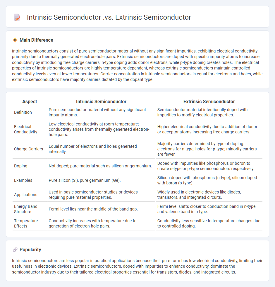
Intrinsic semiconductors consist of pure semiconductor material without any significant impurities, exhibiting electrical conductivity primarily due to thermally generated electron-hole pairs. Extrinsic semiconductors are doped with specific impurity atoms to increase conductivity by introducing free charge carriers; n-type doping adds donor electrons, while p-type doping creates holes. The electrical properties of intrinsic semiconductors are highly temperature-dependent, whereas extrinsic semiconductors maintain controlled conductivity levels even at lower temperatures. Carrier concentration in intrinsic semiconductors is equal for electrons and holes, while extrinsic semiconductors have majority carriers dictated by the dopant type.
Connection
Intrinsic semiconductors consist of pure semiconductor materials like silicon or germanium with no significant impurities, exhibiting balanced electron and hole concentrations. Extrinsic semiconductors are formed by intentionally doping intrinsic materials with impurities, such as phosphorus for n-type or boron for p-type semiconductors, to enhance electrical conductivity. The doping process alters the charge carrier concentration in intrinsic semiconductors, enabling controlled conductivity for electronic device applications.
Comparison Table
| Aspect | Intrinsic Semiconductor | Extrinsic Semiconductor |
|---|---|---|
| Definition | Pure semiconductor material without any significant impurity atoms. | Semiconductor material intentionally doped with impurities to modify electrical properties. |
| Electrical Conductivity | Low electrical conductivity at room temperature; conductivity arises from thermally generated electron-hole pairs. | Higher electrical conductivity due to addition of donor or acceptor atoms increasing free charge carriers. |
| Charge Carriers | Equal number of electrons and holes generated internally. | Majority carriers determined by type of doping: electrons for n-type, holes for p-type; minority carriers are fewer. |
| Doping | Not doped; pure material such as silicon or germanium. | Doped with impurities like phosphorus or boron to create n-type or p-type semiconductors respectively. |
| Examples | Pure silicon (Si), pure germanium (Ge). | Silicon doped with phosphorus (n-type), silicon doped with boron (p-type). |
| Applications | Used in basic semiconductor studies or devices requiring pure material properties. | Widely used in electronic devices like diodes, transistors, and integrated circuits. |
| Energy Band Structure | Fermi level lies near the middle of the band gap. | Fermi level shifts closer to conduction band in n-type and valence band in p-type. |
| Temperature Effects | Conductivity increases with temperature due to generation of electron-hole pairs. | Conductivity less sensitive to temperature changes due to controlled doping. |
Pure Silicon (Intrinsic)
Pure silicon, also known as intrinsic silicon, exhibits a crystalline structure with no intentional doping, resulting in minimal free charge carriers. Its electrical conductivity is governed primarily by thermally generated electron-hole pairs, making it a semiconductor with low intrinsic carrier concentration at room temperature, approximately 1.5 x 10^10 cm^-3. Intrinsic silicon is fundamental in semiconductor engineering, serving as the baseline material for fabricating integrated circuits and photovoltaic cells. The material's purity, typically exceeding 99.9999% (6N silicon), ensures predictable electronic properties essential for advanced microelectronic device performance.
Doping (Extrinsic)
Extrinsic doping in engineering involves intentionally introducing impurities into a semiconductor to modify its electrical properties. Common dopants such as phosphorus or boron are added to silicon to create n-type or p-type materials, enhancing conductivity. Precise control over dopant concentration and distribution determines device performance in applications like transistors and solar cells. Advanced techniques like ion implantation enable accurate doping profiles essential for modern semiconductor fabrication.
Charge Carriers (Electrons & Holes)
Charge carriers in engineering primarily include electrons and holes, crucial for the conduction of electric current in semiconductors. Electrons serve as negative charge carriers, while holes represent the absence of electrons acting as positive carriers, enabling charge transport within materials like silicon. The behavior and concentration of these carriers directly impact the electrical properties and performance of semiconductor devices, including diodes and transistors. Precise control over electron and hole dynamics advances the development of integrated circuits and electronic engineering applications.
Conductivity Control
Conductivity control in engineering involves regulating the electrical conductivity of fluids or materials to ensure optimal performance in systems such as cooling towers, boilers, and water treatment plants. Precise conductivity measurement helps detect impurities, prevent corrosion, scaling, and maintain the efficiency of industrial processes. Advanced sensors use electrochemical principles to provide real-time data, enabling automated adjustments to maintain target conductivity levels. Effective conductivity control reduces maintenance costs and enhances the lifespan of equipment in sectors like power generation and chemical manufacturing.
Applications (Diodes, Transistors)
Diodes and transistors serve critical roles in engineering applications across electronics and communication systems. Diodes enable current flow in one direction, extensively used in rectifiers, voltage regulators, and signal demodulation. Transistors function as switches and amplifiers in circuits, fundamental to digital computing, power control, and RF signal processing. Their integration advances device miniaturization, energy efficiency, and high-speed data transmission technologies.
Source and External Links
What's the difference between an Intrinsic and Extrinsic ... - Intrinsic semiconductors are pure materials with equal numbers of electrons and holes, while extrinsic semiconductors are doped to increase conductivity by altering the balance of charge carriers and shifting the Fermi energy level.
Distinguish Between Intrinsic and Extrinsic Semiconductor - Intrinsic semiconductors depend on thermally generated electron-hole pairs for conductivity and have no added impurities, whereas extrinsic semiconductors are intentionally doped to introduce extra electrons or holes, resulting in much higher and more controllable conductivity.
Intrinsic Semiconductors and Extrinsic Semiconductors - Intrinsic semiconductors are exceedingly pure (e.g., silicon, germanium) with minimal conductivity at room temperature, while extrinsic semiconductors contain deliberate impurities (dopants) that significantly enhance conductivity and create n-type or p-type materials.
FAQs
What is an intrinsic semiconductor?
An intrinsic semiconductor is a pure semiconductor material with equal numbers of electrons and holes, exhibiting electrical conductivity due to thermally generated charge carriers.
What is an extrinsic semiconductor?
An extrinsic semiconductor is a semiconductor material doped with impurities to increase its electrical conductivity by adding free charge carriers.
How are intrinsic and extrinsic semiconductors different?
Intrinsic semiconductors are pure materials with electrical conductivity determined solely by their own electrons and holes, while extrinsic semiconductors are doped with impurities to increase conductivity by introducing additional charge carriers.
What materials are used for intrinsic semiconductors?
Intrinsic semiconductors are primarily made from pure elements like silicon (Si) and germanium (Ge).
How is doping used in extrinsic semiconductors?
Doping in extrinsic semiconductors involves intentionally introducing impurity atoms, such as phosphorus or boron, into the intrinsic semiconductor to increase its electrical conductivity by creating free charge carriers--electrons for n-type doping and holes for p-type doping.
What are the types of extrinsic semiconductors?
The types of extrinsic semiconductors are n-type, which is doped with pentavalent impurities like phosphorus, and p-type, which is doped with trivalent impurities like boron.
Why are extrinsic semiconductors important in electronics?
Extrinsic semiconductors are important in electronics because they provide controlled electrical conductivity through intentional doping, enabling the precise operation of devices like diodes, transistors, and integrated circuits.