Forward bias occurs when the positive terminal of a power source is connected to the p-type semiconductor and the negative terminal to the n-type, allowing current to flow easily across the junction. Reverse bias involves connecting the positive terminal to the n-type and the negative terminal to the p-type, which widens the depletion region and inhibits current flow. Explore further to understand how these biases impact diode and transistor behavior in electronic circuits.
Main Difference
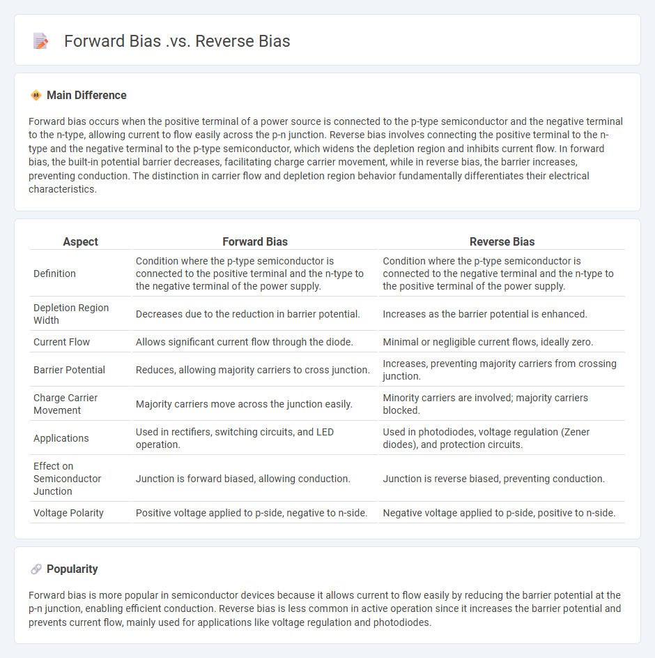
Forward bias occurs when the positive terminal of a power source is connected to the p-type semiconductor and the negative terminal to the n-type, allowing current to flow easily across the p-n junction. Reverse bias involves connecting the positive terminal to the n-type and the negative terminal to the p-type semiconductor, which widens the depletion region and inhibits current flow. In forward bias, the built-in potential barrier decreases, facilitating charge carrier movement, while in reverse bias, the barrier increases, preventing conduction. The distinction in carrier flow and depletion region behavior fundamentally differentiates their electrical characteristics.
Connection
Forward bias and reverse bias describe how voltage applied to a semiconductor diode influences current flow. Forward bias reduces the barrier potential, allowing charge carriers to cross the p-n junction and conduct current, whereas reverse bias increases the barrier potential, inhibiting charge carrier movement and minimizing current flow. These opposing voltage conditions control diode behavior in electronic circuits, enabling functions such as rectification and signal modulation.
Comparison Table
| Aspect | Forward Bias | Reverse Bias |
|---|---|---|
| Definition | Condition where the p-type semiconductor is connected to the positive terminal and the n-type to the negative terminal of the power supply. | Condition where the p-type semiconductor is connected to the negative terminal and the n-type to the positive terminal of the power supply. |
| Depletion Region Width | Decreases due to the reduction in barrier potential. | Increases as the barrier potential is enhanced. |
| Current Flow | Allows significant current flow through the diode. | Minimal or negligible current flows, ideally zero. |
| Barrier Potential | Reduces, allowing majority carriers to cross junction. | Increases, preventing majority carriers from crossing junction. |
| Charge Carrier Movement | Majority carriers move across the junction easily. | Minority carriers are involved; majority carriers blocked. |
| Applications | Used in rectifiers, switching circuits, and LED operation. | Used in photodiodes, voltage regulation (Zener diodes), and protection circuits. |
| Effect on Semiconductor Junction | Junction is forward biased, allowing conduction. | Junction is reverse biased, preventing conduction. |
| Voltage Polarity | Positive voltage applied to p-side, negative to n-side. | Negative voltage applied to p-side, positive to n-side. |
Junction Voltage
Junction voltage refers to the potential difference across the p-n junction in semiconductor devices such as diodes and transistors. It plays a crucial role in determining the current flow and switching characteristics of these components. In silicon diodes, the typical forward junction voltage is approximately 0.7 volts, while gallium arsenide devices may exhibit lower voltages around 0.3 volts. Accurate control and measurement of junction voltage are essential for optimizing device performance in integrated circuits and power electronics.
Current Direction
The field of engineering is rapidly advancing with a strong emphasis on sustainable design and renewable energy technologies. Innovations in artificial intelligence and automation are transforming manufacturing processes and infrastructure development. Civil engineering projects increasingly incorporate smart materials and Internet of Things (IoT) systems to enhance efficiency and resilience. The integration of advanced computational methods and simulation tools is accelerating product development cycles across all engineering disciplines.
Depletion Region
The depletion region in semiconductor engineering refers to the area around the p-n junction where mobile charge carriers are depleted, creating a zone devoid of free electrons and holes. This region forms an electric field that acts as a barrier to charge carrier movement, crucial for diode operation and transistor switching. Its width varies with doping concentration and applied voltage, typically measured in nanometers to micrometers. Control of the depletion region enables precise manipulation of current flow in electronic devices.
Diode Conductivity
Diode conductivity is a fundamental characteristic in semiconductor engineering, describing the ability of a diode to allow current flow primarily in one direction. This property results from the p-n junction within the diode, where electrons and holes recombine, enabling current conduction under forward bias while blocking it under reverse bias. Silicon diodes typically exhibit a forward voltage drop of approximately 0.7 volts, influencing circuit design and efficiency. Understanding diode conductivity parameters such as forward voltage, reverse leakage current, and breakdown voltage is critical for optimizing electronic devices and power systems.
Breakdown Voltage
Breakdown voltage is the critical voltage at which an insulating material becomes electrically conductive, leading to dielectric failure. It varies significantly depending on the material properties, thickness, and environmental conditions such as temperature and humidity. Common breakdown voltages range from a few volts in semiconductors to several million volts in high-voltage transmission insulation. Engineers use breakdown voltage to design reliable electrical components and ensure safety in power systems and electronic devices.
Source and External Links
Forward Bias, Reverse Bias and their effects on Diodes - Wevolver - Forward bias occurs when the anode is at a higher voltage than the cathode, reducing the depletion region and potential barrier to allow current flow, while reverse bias happens when the cathode is at a higher voltage, widening the depletion region and preventing current flow except for a very small leakage current.
PN Junction Reverse Bias versus Forward Bias and Their Functional Characteristics - Cadence - Forward bias decreases a diode's resistance allowing significant current flow by reducing the potential barrier, whereas reverse bias increases the resistance, significantly impeding current flow and thickening the depletion layer.
Diode operation - Energy Education - Forward bias allows current to flow easily through the diode by applying voltage that reduces the barrier, while reverse bias applies voltage in the opposite direction, increasing the depletion region and effectively stopping current flow, which is useful for converting AC to DC and signal manipulation.
FAQs
What is forward bias in a diode?
Forward bias in a diode occurs when the positive terminal of the power source is connected to the diode's anode and the negative terminal to the cathode, reducing the depletion region and allowing current to flow through the diode.
What is reverse bias in a diode?
Reverse bias in a diode occurs when the positive terminal of the power supply is connected to the cathode and the negative terminal to the anode, preventing current flow except a minimal leakage current.
How does current flow in forward bias?
Current flows in forward bias as electrons move from the n-type region to the p-type region and holes move from the p-type region to the n-type region, allowing charge carriers to cross the junction and create electric current.
How does current flow in reverse bias?
In reverse bias, current flow occurs due to minority charge carriers overcoming the depletion region, resulting in a small leakage current called reverse saturation current.
What happens to the depletion layer in forward bias?
The depletion layer in forward bias narrows as the applied voltage reduces the built-in potential barrier, allowing charge carriers to cross the junction more easily.
What happens to the depletion layer in reverse bias?
The depletion layer in reverse bias widens as the applied voltage increases, increasing the barrier potential and reducing current flow.
Why are forward bias and reverse bias important in electronics?
Forward bias enables current flow through semiconductor devices by reducing the potential barrier, while reverse bias prevents current flow, allowing control of electron movement essential for diodes, transistors, and circuit function.