Microfabrication involves the construction of devices and structures at the micrometer scale, typically ranging from 1 to 100 micrometers, using techniques such as photolithography and etching. Nanofabrication operates at a smaller scale, usually below 100 nanometers, employing methods like electron beam lithography and molecular self-assembly to create features with atomic precision. Explore the detailed differences and applications of microfabrication and nanofabrication to understand their impact on modern technology.
Main Difference
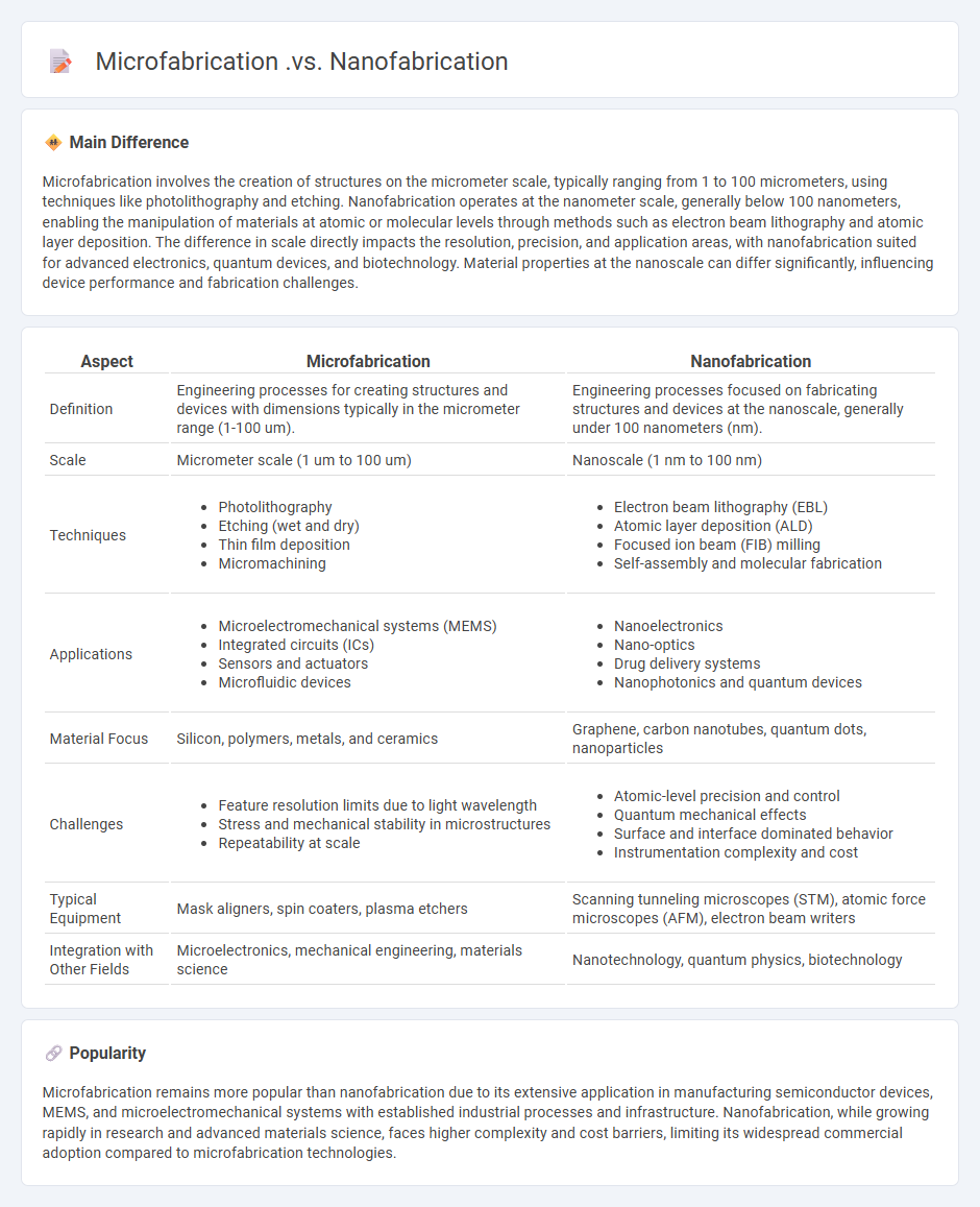
Microfabrication involves the creation of structures on the micrometer scale, typically ranging from 1 to 100 micrometers, using techniques like photolithography and etching. Nanofabrication operates at the nanometer scale, generally below 100 nanometers, enabling the manipulation of materials at atomic or molecular levels through methods such as electron beam lithography and atomic layer deposition. The difference in scale directly impacts the resolution, precision, and application areas, with nanofabrication suited for advanced electronics, quantum devices, and biotechnology. Material properties at the nanoscale can differ significantly, influencing device performance and fabrication challenges.
Connection
Microfabrication and nanofabrication are interconnected through their shared goal of creating structures at extremely small scales, with microfabrication focusing on features typically between 1 to 100 micrometers and nanofabrication targeting dimensions below 100 nanometers. Both utilize advanced lithography, etching, and deposition techniques to achieve precise patterning for applications in microelectronics, MEMS, and nanotechnology. The convergence of these fields enables the development of devices with enhanced performance and functionality by integrating micro- and nanoscale components.
Comparison Table
| Aspect | Microfabrication | Nanofabrication |
|---|---|---|
| Definition | Engineering processes for creating structures and devices with dimensions typically in the micrometer range (1-100 um). | Engineering processes focused on fabricating structures and devices at the nanoscale, generally under 100 nanometers (nm). |
| Scale | Micrometer scale (1 um to 100 um) | Nanoscale (1 nm to 100 nm) |
| Techniques |
|
|
| Applications |
|
|
| Material Focus | Silicon, polymers, metals, and ceramics | Graphene, carbon nanotubes, quantum dots, nanoparticles |
| Challenges |
|
|
| Typical Equipment | Mask aligners, spin coaters, plasma etchers | Scanning tunneling microscopes (STM), atomic force microscopes (AFM), electron beam writers |
| Integration with Other Fields | Microelectronics, mechanical engineering, materials science | Nanotechnology, quantum physics, biotechnology |
Feature Size Resolution
Feature size resolution in engineering refers to the minimum dimension of a physical structure that can be accurately fabricated or measured in manufacturing and microfabrication processes. It is critically important in semiconductor engineering, where advanced photolithography techniques achieve resolutions below 5 nanometers to support the production of high-performance integrated circuits. In precision machining and additive manufacturing, resolution determines the accuracy and surface finish of components, often measured in micrometers or even nanometers for cutting-edge applications. Advances in feature size resolution drive improvements in electronics, MEMS devices, and nanoscale engineering by enabling smaller, faster, and more efficient systems.
Lithography Methods
Lithography methods are critical in modern engineering for fabricating micro- and nanoscale structures on semiconductor wafers. Techniques such as photolithography, electron beam lithography, and nanoimprint lithography enable precise patterning with features as small as 5 nanometers. Photolithography dominates the semiconductor industry, utilizing ultraviolet light and photomasks to transfer circuit designs onto silicon substrates. Emerging methods focus on enhancing resolution and throughput to support next-generation integrated circuits and flexible electronics manufacturing.
Material Deposition Techniques
Material deposition techniques in engineering encompass advanced methods such as chemical vapor deposition (CVD), physical vapor deposition (PVD), and atomic layer deposition (ALD). These processes enable precise layering of materials at the micro and nanoscale, essential for fabricating semiconductors, thin films, and coatings with enhanced mechanical and electrical properties. Industrial applications leverage these techniques to improve the durability, conductivity, and corrosion resistance of engineered components across aerospace, automotive, and electronics sectors. Optimizing parameters like temperature, pressure, and precursor materials during deposition ensures high-quality, uniform films critical for next-generation device performance.
Device Application Scale
Device application scale in engineering refers to the size and scope at which devices are designed and implemented, ranging from micro-scale components like MEMS (Micro-Electro-Mechanical Systems) to large industrial machinery. Scaling impacts performance parameters such as power consumption, thermal management, and material properties, necessitating precise engineering techniques for each scale. Engineers utilize simulation tools and fabrication technologies to optimize device behavior for specific applications, ensuring reliability and efficiency. Advances in nanotechnology and additive manufacturing continue to push the boundaries of device application scales across various engineering disciplines.
Cleanroom Requirements
Cleanroom requirements in engineering specify controlled environments with low levels of pollutants such as dust, airborne microbes, aerosol particles, and chemical vapors. These specifications often include ISO 14644 standards, which categorize cleanrooms from ISO Class 1 (cleanest) to ISO Class 9 (least clean), based on particle concentration limits per cubic meter. Cleanroom design mandates precise control of temperature, humidity, airflow, and filtration systems, typically employing HEPA or ULPA filters to maintain air purity. Compliance with these requirements supports manufacturing processes in semiconductor, pharmaceutical, and aerospace industries, where contamination adversely impacts product quality and functionality.
Source and External Links
## Set 1Micro- and nanofabrication methods in nanotechnological medical applications - This article discusses how micro- and nanofabrication techniques are applied in medical devices, particularly in point-of-care diagnostics.
## Set 2Microfabrication and Nanofabrication: Precision Manufacturing - This book explores the intersection of micro and nano fabrication techniques, detailing their role in precision manufacturing and their potential to revolutionize conventional production methods.
## Set 3Introduction to Micro-/Nanofabrication - This chapter provides an overview of key micro- and nanofabrication techniques, including those borrowed from the semiconductor industry and used for various applications.
FAQs
What is microfabrication?
Microfabrication is the process of constructing microscopic structures and devices on a substrate, typically used in semiconductor manufacturing, MEMS, and nanotechnology.
What defines nanofabrication?
Nanofabrication is the process of designing and creating structures, devices, and systems at the nanometer scale, typically ranging from 1 to 100 nanometers, using techniques such as electron-beam lithography, nanoimprint lithography, and atomic layer deposition.
How do microfabrication and nanofabrication differ in scale?
Microfabrication involves structures sized from 1 micrometer (um) to several hundred micrometers, while nanofabrication focuses on features at the nanometer scale, typically below 100 nanometers (nm).
What materials are used in microfabrication and nanofabrication?
Microfabrication and nanofabrication primarily use silicon, photoresists, metals like gold, aluminum, and copper, dielectric materials such as silicon dioxide and silicon nitride, polymers like SU-8 and PDMS, as well as advanced 2D materials including graphene and molybdenum disulfide.
What are common techniques in microfabrication and nanofabrication?
Common microfabrication techniques include photolithography, etching (wet and dry), chemical vapor deposition (CVD), physical vapor deposition (PVD), and doping; nanofabrication techniques include electron beam lithography, nanoimprint lithography, atomic layer deposition (ALD), focused ion beam (FIB) milling, and self-assembly methods.
What applications rely on microfabrication versus nanofabrication?
Microfabrication is primarily used in applications like MEMS devices, microfluidics, integrated circuits, and sensors, while nanofabrication is essential for quantum dots, nanoscale transistors, molecular electronics, and advanced photonics.
What are the main challenges in microfabrication and nanofabrication?
Main challenges in microfabrication and nanofabrication include achieving precise patterning at atomic scales, controlling material properties and defects, minimizing feature size variability, ensuring high throughput and scalability, integrating diverse materials, managing contamination and surface roughness, and developing cost-effective, reliable fabrication techniques.