VLSI design involves creating integrated circuits by combining thousands of transistors into a single chip, focusing on scalability and system-level integration. ASIC design, a subset of VLSI, targets customized application-specific chips optimized for performance, power, and area for particular tasks. Explore the detailed distinctions and applications of VLSI and ASIC design to enhance your semiconductor knowledge.
Main Difference
VLSI design focuses on creating very large-scale integrated circuits that can include a wide range of functionalities and are used in various applications such as microprocessors, memory chips, and digital signal processors. ASIC design, a subset of VLSI, involves designing chips customized for a specific application, optimizing performance, power, and area for a dedicated function. VLSI design is broader, encompassing both general-purpose and application-specific integrated circuits, while ASIC design targets specialized hardware solutions. The design process for ASICs often requires extensive verification and testing tailored to the specific use case to ensure reliability and efficiency.
Connection
VLSI design encompasses the process of creating integrated circuits by combining thousands of transistors into a single chip, forming the foundation for ASIC design. ASIC design specifically focuses on developing application-specific integrated circuits tailored for particular functions or applications, utilizing VLSI methodologies to optimize performance and power efficiency. The synergy between VLSI and ASIC design enables custom hardware solutions that meet unique system requirements with enhanced speed and reduced silicon area.
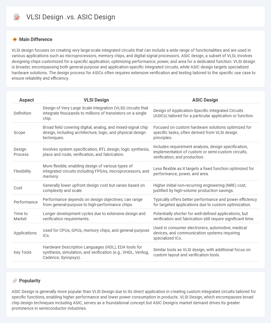
Comparison Table
| Aspect | VLSI Design | ASIC Design |
|---|---|---|
| Definition | Design of Very Large Scale Integration (VLSI) circuits that integrate thousands to millions of transistors on a single chip. | Design of Application-Specific Integrated Circuits (ASICs) tailored for a particular application or function. |
| Scope | Broad field covering digital, analog, and mixed-signal chip design, including architecture, logic, and physical design techniques. | Focused on custom hardware solutions optimized for specific tasks, often derived from VLSI design principles. |
| Design Process | Involves system specification, RTL design, logic synthesis, place and route, verification, and fabrication. | Includes requirement analysis, design specification, implementation of custom or semi-custom circuits, verification, and production. |
| Flexibility | More flexible, enabling design of various types of integrated circuits including FPGAs, microprocessors, and memory. | Less flexible as it targets a fixed function optimized for performance, power, and area. |
| Cost | Generally lower upfront design cost but varies based on complexity and scale. | Higher initial non-recurring engineering (NRE) cost, justified by high-volume production savings. |
| Performance | Performance depends on design objectives; can range from general-purpose to high-performance chips. | Typically offers better performance and power efficiency for targeted applications due to custom optimization. |
| Time to Market | Longer development cycles due to extensive design and verification requirements. | Potentially shorter for well-defined applications, but verification and fabrication still require significant time. |
| Applications | Used for CPUs, GPUs, memory chips, and general-purpose ICs. | Used in consumer electronics, automotive, medical devices, and communication systems requiring specialized ICs. |
| Key Tools | Hardware Description Languages (HDL), EDA tools for synthesis, simulation, and verification (e.g., VHDL, Verilog, Cadence, Synopsys). | Similar tools as VLSI design, with additional focus on custom layout and verification tools. |
VLSI (Very Large Scale Integration)
VLSI (Very Large Scale Integration) refers to the process of integrating thousands to millions of transistors onto a single silicon chip to create complex electronic circuits. This technology enables the fabrication of microprocessors, memory chips, and application-specific integrated circuits (ASICs) used in modern computing devices. Advanced lithography techniques and CAD tools play critical roles in the design and manufacturing of VLSI circuits, achieving high-density integration and improved performance. The evolution of VLSI has driven innovations in consumer electronics, telecommunications, and automotive systems worldwide.
ASIC (Application-Specific Integrated Circuit)
ASICs (Application-Specific Integrated Circuits) are customized semiconductor devices designed to perform specialized tasks within electronic systems. These circuits enhance performance and energy efficiency by integrating specific functions, unlike general-purpose processors. Commonly used in telecommunications, automotive systems, and consumer electronics, ASICs enable faster processing speeds and reduced power consumption. The design process involves hardware description languages (HDLs) and advanced fabrication technologies to optimize functionality and scalability.
Design Methodology
Design methodology in engineering involves systematic approaches to developing solutions, integrating principles of analysis, synthesis, and optimization. Emphasis is placed on iterative prototyping, simulation, and validation techniques to enhance product reliability and performance. Established frameworks such as the V-Model and Agile methodologies guide project phases from concept to deployment. Advanced tools like CAD software and finite element analysis support precision and efficiency throughout the design process.
Customization Level
Customization level in engineering refers to the degree to which products or systems are tailored to meet specific client requirements or operational needs. High customization levels often involve modifying design parameters, selecting specialized materials, or integrating bespoke components to optimize performance and functionality. Engineers employ advanced software tools like CAD and CAE to simulate and refine customized solutions, ensuring precision and feasibility. Balancing customization with cost-efficiency is critical in sectors such as aerospace, automotive, and industrial manufacturing.
Application Domain
Application domain in engineering encompasses fields where engineering principles and technologies are applied to design, develop, and optimize systems, structures, and processes. Key sectors include civil engineering for infrastructure, mechanical engineering for machinery and manufacturing, electrical engineering for power and electronics, and software engineering for creating applications and embedded systems. Emerging domains such as renewable energy, robotics, and biomedical engineering are rapidly advancing with innovations focused on sustainability, automation, and healthcare technology. Engineers utilize computer-aided design (CAD), simulation software, and data analytics to enhance precision and efficiency across these diverse application domains.
Source and External Links
## Topic: VLSI DesignExplained FPGA vs ASIC in VLSI - VLSI (Very Large-Scale Integration) refers to the process of creating integrated circuits by combining thousands to billions of transistors into a single chip, encompassing both ASIC and FPGA design methodologies.
## Topic: ASIC DesignASIC vs. FPGA: What's the difference? - ASIC (Application-Specific Integrated Circuit) design is a VLSI approach where chips are custom-designed and optimized for a specific application, offering superior performance, efficiency, and cost-effectiveness at high volumes, but with higher upfront costs and longer development cycles.
## Topic: ComparisonASIC vs. FPGA in VLSI: Understanding the Differences - While VLSI is the broader field of integrating complex circuits, ASIC design within VLSI focuses on custom, non-reprogrammable chips for mass production, whereas FPGA design emphasizes flexibility and reprogrammability for prototyping and low-volume applications.
FAQs
What is VLSI design?
VLSI design refers to the process of creating integrated circuits by combining thousands to millions of transistors on a single silicon chip to achieve complex electronic functions.
What is ASIC design?
ASIC design is the process of creating customized Integrated Circuits optimized for specific applications by defining their functionality, architecture, and layout to achieve high performance and efficiency.
How does VLSI differ from ASIC design?
VLSI (Very Large Scale Integration) refers to the process of creating integrated circuits by combining thousands to millions of transistors on a single chip, while ASIC (Application-Specific Integrated Circuit) design focuses on creating custom chips optimized for a specific application or task within the VLSI framework.
What are the main steps in VLSI design?
The main steps in VLSI design are system specification, architectural design, RTL coding, logic synthesis, design verification, physical design (floorplanning, placement, routing), timing analysis, and design for testability.
What technologies are used in ASIC design?
ASIC design utilizes technologies including CMOS process technology, hardware description languages (HDLs) like VHDL and Verilog, electronic design automation (EDA) tools, standard cell libraries, and design for testability (DFT) techniques.
What are the advantages of VLSI over ASIC design?
VLSI offers greater flexibility, reprogrammability, shorter development time, and lower non-recurring engineering (NRE) costs compared to ASIC design.
When should you choose ASIC instead of VLSI design?
Choose ASIC over VLSI design when you require a custom, high-performance, low-power, and cost-effective solution for high-volume production with fixed functionality.