VLSI design focuses on creating integrated circuits by fabricating custom silicon chips for specific applications, emphasizing high performance and low power consumption in products like processors and memory devices. FPGA design utilizes field-programmable gate arrays to develop flexible hardware that can be reprogrammed after manufacturing, ideal for prototyping and adaptable systems. Explore the detailed differences and benefits of VLSI and FPGA design to determine the best approach for your project.
Main Difference
VLSI design focuses on creating custom integrated circuits by defining transistor-level layouts for large-scale, high-performance chips, while FPGA design involves configuring pre-fabricated, reprogrammable hardware blocks to implement digital circuits rapidly. VLSI demands extensive fabrication processes and longer development cycles, aiming for optimized power, area, and speed at the silicon level. FPGA design benefits from flexibility and shorter time-to-market, enabling iterative testing and modifications without physical chip fabrication. Advanced EDA tools support both design flows, but VLSI targets ASIC production, whereas FPGA emphasizes dynamic hardware configurability.
Connection
VLSI design involves the creation of integrated circuits by combining thousands to millions of transistors on a single chip, while FPGA design focuses on programming configurable logic blocks within Field Programmable Gate Arrays to implement custom hardware functions. Both domains rely heavily on hardware description languages such as VHDL or Verilog for modeling and simulating digital circuits at the register-transfer level. VLSI methodologies influence FPGA architecture and design techniques, enabling optimized circuit performance, reduced power consumption, and rapid prototyping of complex systems.
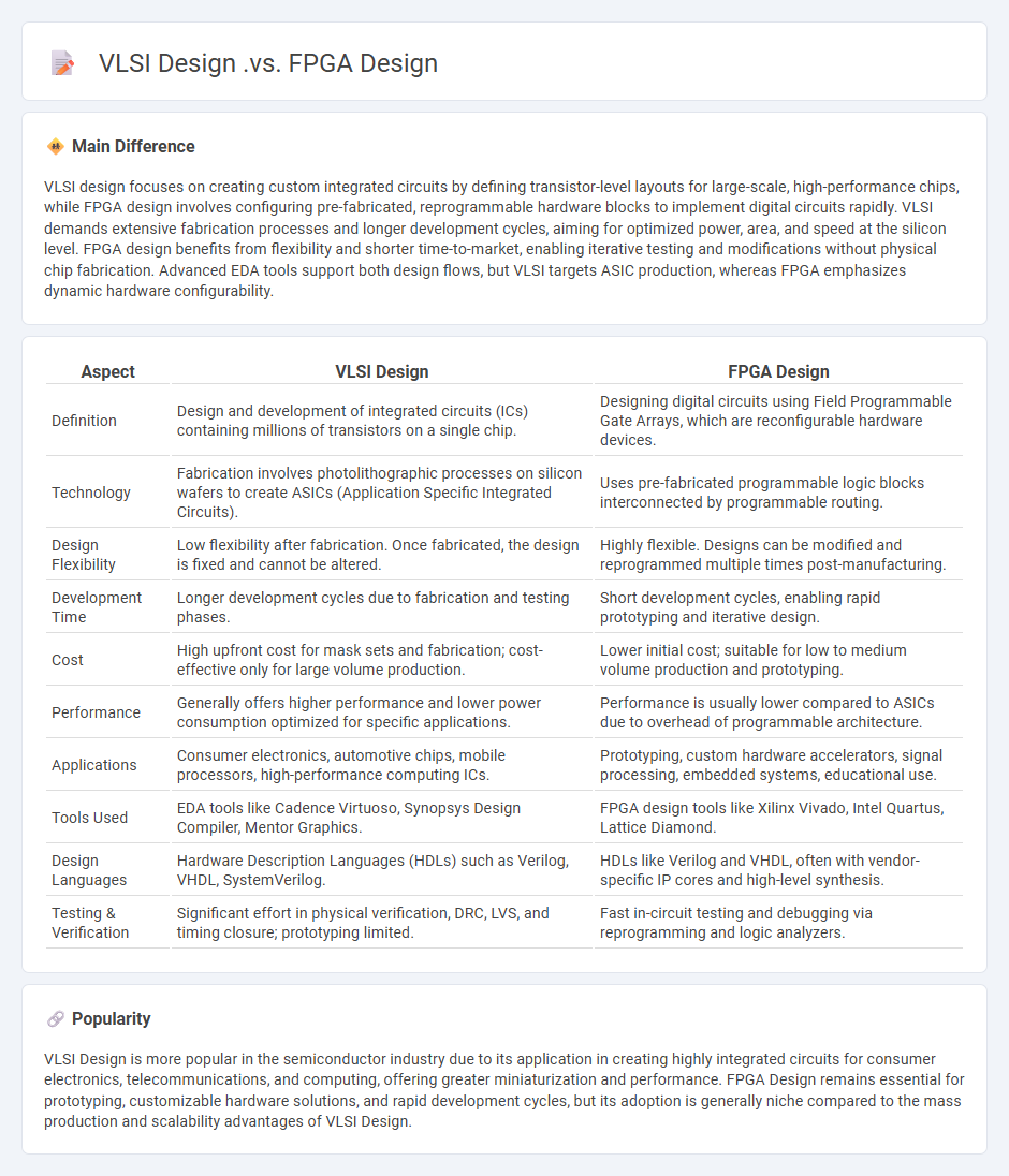
Comparison Table
| Aspect | VLSI Design | FPGA Design |
|---|---|---|
| Definition | Design and development of integrated circuits (ICs) containing millions of transistors on a single chip. | Designing digital circuits using Field Programmable Gate Arrays, which are reconfigurable hardware devices. |
| Technology | Fabrication involves photolithographic processes on silicon wafers to create ASICs (Application Specific Integrated Circuits). | Uses pre-fabricated programmable logic blocks interconnected by programmable routing. |
| Design Flexibility | Low flexibility after fabrication. Once fabricated, the design is fixed and cannot be altered. | Highly flexible. Designs can be modified and reprogrammed multiple times post-manufacturing. |
| Development Time | Longer development cycles due to fabrication and testing phases. | Short development cycles, enabling rapid prototyping and iterative design. |
| Cost | High upfront cost for mask sets and fabrication; cost-effective only for large volume production. | Lower initial cost; suitable for low to medium volume production and prototyping. |
| Performance | Generally offers higher performance and lower power consumption optimized for specific applications. | Performance is usually lower compared to ASICs due to overhead of programmable architecture. |
| Applications | Consumer electronics, automotive chips, mobile processors, high-performance computing ICs. | Prototyping, custom hardware accelerators, signal processing, embedded systems, educational use. |
| Tools Used | EDA tools like Cadence Virtuoso, Synopsys Design Compiler, Mentor Graphics. | FPGA design tools like Xilinx Vivado, Intel Quartus, Lattice Diamond. |
| Design Languages | Hardware Description Languages (HDLs) such as Verilog, VHDL, SystemVerilog. | HDLs like Verilog and VHDL, often with vendor-specific IP cores and high-level synthesis. |
| Testing & Verification | Significant effort in physical verification, DRC, LVS, and timing closure; prototyping limited. | Fast in-circuit testing and debugging via reprogramming and logic analyzers. |
ASIC (Application-Specific Integrated Circuit)
ASIC (Application-Specific Integrated Circuit) refers to a type of integrated circuit customized for a particular use rather than general-purpose applications. These circuits are designed to optimize performance, power consumption, and area efficiency for specific engineering tasks such as telecommunications, automotive systems, and consumer electronics. Leading semiconductor companies like TSMC and Samsung manufacture ASICs using advanced process nodes, including 5nm and 3nm technologies, enabling faster speeds and lower power dissipation. ASICs play a critical role in industries requiring high performance and low latency, such as cryptocurrency mining, 5G infrastructure, and IoT devices.
Programmability
Programmability in engineering refers to the ability of systems, devices, or machines to be configured or controlled through software instructions to perform specific tasks or functions. It enables customization, automation, and flexibility in engineering processes, enhancing efficiency and adaptability across various applications such as robotics, embedded systems, and manufacturing. Modern programmable logic controllers (PLCs) and microcontrollers are key components driving advancements in industrial automation and smart technologies. Effective programmability reduces human error and accelerates prototyping and production cycles in engineering projects.
Design Flow
Design flow in engineering refers to the structured sequence of stages involved in the development of a product or system, encompassing concept generation, detailed design, prototyping, testing, and manufacturing. It incorporates methodologies such as systems engineering, CAD modeling, simulation, and verification to ensure functional and performance requirements are met efficiently. Key tools include software like AutoCAD, SolidWorks, and MATLAB for design and analysis, facilitating iteration and optimization within tight project timelines. Effective design flow reduces discovery of errors in later stages, minimizes costs, and accelerates time-to-market for engineering solutions.
Time-to-Market
Time-to-Market (TTM) in engineering measures the duration from product conception to its availability for sale, directly influencing competitive advantage. Optimizing TTM involves streamlined project management, rapid prototyping, and agile development methodologies to reduce delays and costs. Engineers leverage digital tools like CAD software and simulation to accelerate design cycles and enhance precision. Efficient supply chain coordination and concurrent engineering processes further shorten TTM, enabling quicker response to market demands.
Career Pathways
Career pathways in engineering encompass diverse specializations such as civil, mechanical, electrical, and software engineering, each requiring specific technical skills and certifications. Engineers often pursue professional development through programs like the Fundamentals of Engineering (FE) exam and Professional Engineer (PE) licensure to advance their careers. Emerging fields like renewable energy engineering and artificial intelligence engineering are experiencing significant growth, driven by technological innovation and sustainability demands. Strong analytical abilities, proficiency in computer-aided design (CAD) software, and project management expertise are critical for engineers to succeed in competitive markets.
Source and External Links
What is an FPGA in VLSI? - ChipEdge - FPGA in VLSI is a reprogrammable integrated circuit made of Configurable Logic Blocks that enables parallel computing and flexibility, whereas VLSI design broadly refers to creating custom integrated circuits like ASICs that are optimized for specific applications.
ASIC vs. FPGA in VLSI: Understanding the Differences ... - YouTube - FPGA designs are flexible and reprogrammable with shorter production times and are preferred for prototyping, while ASICs (custom VLSI designs) have higher design complexity, longer time to market, better performance, and are suited for fixed, optimized applications.
ASIC vs. FPGA: What's the difference? | ASIC North Inc - ASIC is a custom, non-reprogrammable chip designed for a specific application with optimized performance and cost for large volumes, while FPGA is a multipurpose, reprogrammable chip suitable for various applications and frequent upgrades in design.
FAQs
What is VLSI design?
VLSI design is the process of creating integrated circuits by combining thousands to millions of transistors onto a single chip.
What is FPGA design?
FPGA design is the process of creating and programming field-programmable gate arrays to implement custom digital circuits for specific applications.
How do VLSI and FPGA differ in implementation?
VLSI involves designing custom integrated circuits with fixed hardware logic, while FPGA uses programmable logic blocks and interconnects to implement configurable hardware designs.
What applications use VLSI versus FPGA?
VLSI is used in high-volume, performance-critical applications like microprocessors, ASICs for smartphones, and custom integrated circuits, while FPGAs are preferred for flexible, low-to-medium volume uses such as prototyping, telecommunications, aerospace, and adaptive signal processing.
Which offers better performance, VLSI or FPGA?
VLSI offers better performance than FPGA due to its custom hardware design and lower latency.
How does the development process differ between VLSI and FPGA?
VLSI development involves custom silicon design with longer fabrication cycles and higher non-recurring engineering costs, whereas FPGA development uses pre-manufactured programmable logic devices enabling rapid prototyping and iterative design changes without fabrication.
What are the cost implications of VLSI and FPGA design?
VLSI design incurs high initial costs due to expensive fabrication, mask generation, and longer development cycles, while FPGA design offers lower upfront costs with reusable hardware and shorter time-to-market but generally higher per-unit costs in large-scale production.