Polycrystalline silicon consists of multiple small silicon crystals, offering cost-effective production and moderate efficiency in solar panels. Monocrystalline silicon features a single continuous crystal structure, delivering higher efficiency and better performance in limited space. Explore the differences in technology and applications to determine which silicon type suits your energy needs.
Main Difference
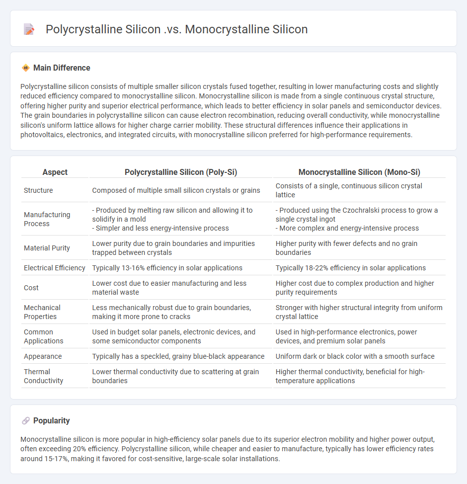
Polycrystalline silicon consists of multiple smaller silicon crystals fused together, resulting in lower manufacturing costs and slightly reduced efficiency compared to monocrystalline silicon. Monocrystalline silicon is made from a single continuous crystal structure, offering higher purity and superior electrical performance, which leads to better efficiency in solar panels and semiconductor devices. The grain boundaries in polycrystalline silicon can cause electron recombination, reducing overall conductivity, while monocrystalline silicon's uniform lattice allows for higher charge carrier mobility. These structural differences influence their applications in photovoltaics, electronics, and integrated circuits, with monocrystalline silicon preferred for high-performance requirements.
Connection
Polycrystalline silicon and monocrystalline silicon are connected through their roles in semiconductor and photovoltaic industries, with polycrystalline silicon serving as a cost-effective raw material source for producing monocrystalline silicon wafers. Both materials consist of silicon atoms arranged in different crystalline structures, affecting their electrical efficiency; monocrystalline silicon features a continuous crystal lattice, while polycrystalline silicon contains multiple crystal grains. This structural distinction influences the efficiency of solar cells, where monocrystalline silicon offers higher energy conversion rates, and manufacturing processes often transition from polycrystalline silicon feedstock to refined monocrystalline wafers.
Comparison Table
| Aspect | Polycrystalline Silicon (Poly-Si) | Monocrystalline Silicon (Mono-Si) |
|---|---|---|
| Structure | Composed of multiple small silicon crystals or grains | Consists of a single, continuous silicon crystal lattice |
| Manufacturing Process |
- Produced by melting raw silicon and allowing it to solidify in a mold - Simpler and less energy-intensive process |
- Produced using the Czochralski process to grow a single crystal ingot - More complex and energy-intensive process |
| Material Purity | Lower purity due to grain boundaries and impurities trapped between crystals | Higher purity with fewer defects and no grain boundaries |
| Electrical Efficiency | Typically 13-16% efficiency in solar applications | Typically 18-22% efficiency in solar applications |
| Cost | Lower cost due to easier manufacturing and less material waste | Higher cost due to complex production and higher purity requirements |
| Mechanical Properties | Less mechanically robust due to grain boundaries, making it more prone to cracks | Stronger with higher structural integrity from uniform crystal lattice |
| Common Applications | Used in budget solar panels, electronic devices, and some semiconductor components | Used in high-performance electronics, power devices, and premium solar panels |
| Appearance | Typically has a speckled, grainy blue-black appearance | Uniform dark or black color with a smooth surface |
| Thermal Conductivity | Lower thermal conductivity due to scattering at grain boundaries | Higher thermal conductivity, beneficial for high-temperature applications |
Crystal Structure
Crystal structure defines the ordered arrangement of atoms in a crystalline material, influencing its mechanical, thermal, and electrical properties crucial in engineering applications. Common crystal systems include cubic, tetragonal, hexagonal, and orthorhombic, each with distinct lattice parameters that affect material behavior under stress. Materials like metals often exhibit a face-centered cubic (FCC) or body-centered cubic (BCC) structure, impacting their ductility and strength. Understanding crystal structure enables engineers to tailor materials for specific functions such as aerospace components, semiconductors, and structural frameworks.
Efficiency Rate
Efficiency rate in engineering measures the output performance of a system relative to its input, typically expressed as a percentage. It evaluates how well a machine, device, or process converts energy or resources into useful work, with common examples including thermal efficiency in engines and energy efficiency in electrical motors. High efficiency rates indicate minimal energy loss, optimizing resource utilization and operational cost. Engineering standards often target efficiency improvements to enhance sustainability and system reliability.
Manufacturing Process
The manufacturing process in engineering encompasses a series of operations that transform raw materials into finished products through methods such as casting, machining, welding, and additive manufacturing. Advanced techniques like CNC machining and 3D printing enhance precision and efficiency, reducing material waste and production time. Quality control measures, including statistical process control (SPC) and Six Sigma methodologies, ensure consistent product performance and compliance with engineering standards. Integration of Industry 4.0 technologies, such as IoT sensors and automation, optimizes manufacturing workflows and enables real-time monitoring.
Cost Analysis
Cost analysis in engineering involves evaluating the total expenses associated with a project, including materials, labor, equipment, and overhead costs. Precise cost estimation methods such as parametric costing, activity-based costing, and bottom-up estimating are essential for accurate budgeting and financial planning. Implementing cost control measures throughout the project lifecycle helps minimize waste, optimize resource allocation, and ensure adherence to financial constraints. Advanced software tools like MATLAB and Primavera facilitate detailed cost tracking and forecasting in complex engineering projects.
Durability and Longevity
Engineering materials such as steel and reinforced concrete are designed for high durability, resisting environmental factors like corrosion and wear to ensure structural longevity. Advanced coatings and treatments extend the lifespan of mechanical components, reducing maintenance costs and downtime. Predictive maintenance and material science innovations enhance the reliability and durability of engineering systems, supporting sustainable infrastructure development. Industry standards, such as ASTM and ISO, establish guidelines to measure and assure durability benchmarks in engineering projects.
Source and External Links
Monocrystalline Vs. Polycrystalline Solar Panels (What's Best?) - Monocrystalline panels use a single pure silicon crystal, are more efficient (typically 15-20%), have a black appearance, last longer (25-40 years), and cost more, whereas polycrystalline panels have multiple silicon fragments, are less efficient (13-16%), appear blue, have a shorter lifespan (20-35 years), but are more affordable.
Monocrystalline vs. Polycrystalline Solar Panels - Monocrystalline cells are cut from a single silicon source leading to higher efficiency, while polycrystalline cells are blended from multiple silicon sources and are slightly less efficient; advances like PERC or half-cut cells improve efficiency for both types.
Monocrystalline vs Polycrystalline: Which Solar Panel is Better? - Monocrystalline panels are more space-efficient and perform better in heat and low light, tend to have higher durability and aesthetics, while polycrystalline are cheaper but less efficient and have more heat-related efficiency loss.
FAQs
What is silicon?
Silicon is a chemical element with the symbol Si and atomic number 14, widely used as a semiconductor material in electronics and solar cells.
What is the difference between polycrystalline and monocrystalline silicon?
Monocrystalline silicon consists of a single continuous crystal structure with uniform lattice orientation, offering higher efficiency and better performance in solar cells, while polycrystalline silicon is composed of multiple smaller silicon crystals with grain boundaries, resulting in lower efficiency and reduced manufacturing costs.
How is polycrystalline silicon made?
Polycrystalline silicon is made by chemically purifying metallurgical-grade silicon through the Siemens process, where trichlorosilane gas is decomposed at high temperatures on heated silicon rods, resulting in high-purity silicon deposits that form polycrystalline ingots.
How is monocrystalline silicon made?
Monocrystalline silicon is made by the Czochralski process, which involves melting high-purity silicon in a crucible and slowly pulling a single crystal seed from the molten silicon to form a cylindrical ingot.
Which type of silicon is more efficient in solar panels?
Monocrystalline silicon is more efficient in solar panels, with efficiencies typically around 20-22%, compared to polycrystalline silicon's 15-17%.
What are the main uses of polycrystalline and monocrystalline silicon?
Polycrystalline silicon is mainly used in solar panels and electronics manufacturing, while monocrystalline silicon is primarily utilized in high-efficiency solar cells and semiconductor devices.
Why choose monocrystalline over polycrystalline silicon?
Monocrystalline silicon offers higher efficiency, better space efficiency, longer lifespan, and superior performance in low-light conditions compared to polycrystalline silicon.