Dielectric breakdown occurs when an insulating material suddenly becomes conductive due to a strong electric field causing electron avalanches within the dielectric. Avalanche breakdown specifically refers to the multiplication of charge carriers in a semiconductor or insulator when accelerated electrons collide with atoms, generating additional charge carriers. Explore the detailed mechanisms and applications of dielectric and avalanche breakdown to understand their impact on electronic device performance.
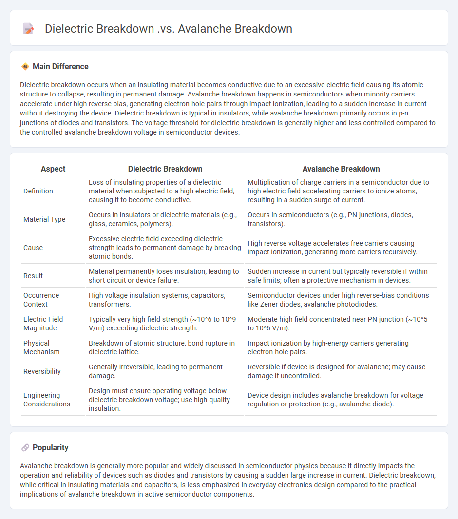
Main Difference
Dielectric breakdown occurs when an insulating material becomes conductive due to an excessive electric field causing its atomic structure to collapse, resulting in permanent damage. Avalanche breakdown happens in semiconductors when minority carriers accelerate under high reverse bias, generating electron-hole pairs through impact ionization, leading to a sudden increase in current without destroying the device. Dielectric breakdown is typical in insulators, while avalanche breakdown primarily occurs in p-n junctions of diodes and transistors. The voltage threshold for dielectric breakdown is generally higher and less controlled compared to the controlled avalanche breakdown voltage in semiconductor devices.
Connection
Dielectric breakdown occurs when an insulating material experiences a critical electric field, causing it to become conductive, while avalanche breakdown happens in semiconductors when carriers gain sufficient kinetic energy to ionize atoms, generating a chain reaction of free carriers. Both phenomena involve the rapid increase of current due to high electric fields surpassing material thresholds, leading to irreversible damage or permanent conductivity. Understanding the relationship between dielectric breakdown and avalanche breakdown is crucial for designing reliable electronic devices and insulating materials that can withstand high voltage stress.
Comparison Table
| Aspect | Dielectric Breakdown | Avalanche Breakdown |
|---|---|---|
| Definition | Loss of insulating properties of a dielectric material when subjected to a high electric field, causing it to become conductive. | Multiplication of charge carriers in a semiconductor due to high electric field accelerating carriers to ionize atoms, resulting in a sudden surge of current. |
| Material Type | Occurs in insulators or dielectric materials (e.g., glass, ceramics, polymers). | Occurs in semiconductors (e.g., PN junctions, diodes, transistors). |
| Cause | Excessive electric field exceeding dielectric strength leads to permanent damage by breaking atomic bonds. | High reverse voltage accelerates free carriers causing impact ionization, generating more carriers recursively. |
| Result | Material permanently loses insulation, leading to short circuit or device failure. | Sudden increase in current but typically reversible if within safe limits; often a protective mechanism in devices. |
| Occurrence Context | High voltage insulation systems, capacitors, transformers. | Semiconductor devices under high reverse-bias conditions like Zener diodes, avalanche photodiodes. |
| Electric Field Magnitude | Typically very high field strength (~10^6 to 10^9 V/m) exceeding dielectric strength. | Moderate high field concentrated near PN junction (~10^5 to 10^6 V/m). |
| Physical Mechanism | Breakdown of atomic structure, bond rupture in dielectric lattice. | Impact ionization by high-energy carriers generating electron-hole pairs. |
| Reversibility | Generally irreversible, leading to permanent damage. | Reversible if device is designed for avalanche; may cause damage if uncontrolled. |
| Engineering Considerations | Design must ensure operating voltage below dielectric breakdown voltage; use high-quality insulation. | Device design includes avalanche breakdown for voltage regulation or protection (e.g., avalanche diode). |
Electric Field Strength
Electric field strength in engineering is measured in volts per meter (V/m) and quantifies the force exerted per unit charge in an electric field. This parameter is crucial for designing insulation systems in high-voltage equipment to prevent dielectric breakdown. Accurate calculation of electric field strength involves factors such as electrode geometry, material permittivity, and voltage magnitude. Engineers use finite element analysis (FEA) software extensively to model and optimize electric field distributions in electrical devices.
Carrier Multiplication
Carrier multiplication in engineering refers to the process where a single high-energy photon generates multiple electron-hole pairs in semiconductor materials. This phenomenon enhances the efficiency of devices like solar cells and photodetectors by increasing the photocurrent beyond conventional limits. Materials such as quantum dots, lead sulfide, and graphene exhibit significant carrier multiplication effects due to their unique electronic properties. Optimizing carrier multiplication can lead to breakthroughs in energy conversion and optoelectronic applications, driving advancements in sustainable technology.
Thermal Runaway
Thermal runaway in engineering refers to a rapid, uncontrolled increase in temperature within a system, often caused by an exothermic reaction or electrical failure. This phenomenon is particularly critical in lithium-ion batteries, where overheating can lead to fires or explosions due to electrolyte decomposition and gas generation. Engineers employ thermal management systems, including cooling mechanisms and thermal sensors, to detect and mitigate thermal runaway risks. Understanding heat transfer processes and material properties is essential for designing safer energy storage devices and electronic components.
Breakdown Voltage
Breakdown voltage represents the critical electric potential at which an insulating material becomes conductive, causing a sudden surge of current. This parameter is essential in designing electrical components such as capacitors, transformers, and semiconductors to prevent failure under high voltage stress. Commonly expressed in volts (V), breakdown voltage varies significantly with material properties and environmental conditions like temperature and humidity. For silicon dioxide, a key insulating material in microelectronics, typical breakdown voltage ranges from 10^7 to 10^8 V/m, highlighting its effectiveness in high-voltage applications.
Ionization Mechanism
Ionization mechanisms in engineering involve processes that generate charged particles by removing or adding electrons to atoms or molecules, crucial for applications like plasma generation and mass spectrometry. Common ionization techniques include electron impact, photoionization, and field ionization, each tailored to specific engineering needs such as materials analysis or semiconductor fabrication. Understanding the ionization energy and cross-section of materials enhances precision in designing sensors and ion sources used in aerospace and chemical engineering. Advances in controlled ionization improve the efficiency of energy conversion systems and environmental monitoring technologies.
Source and External Links
ROHINI COLLEGE OF ENGINEERING AND TECHNOLOGY - Dielectric breakdown (intrinsic/avalanche) occurs in insulating materials due to a large electric field, causing a sudden, large current flow, while avalanche breakdown in semiconductors involves a chain reaction of collisions that multiplies charge carriers under sufficient reverse bias.
Difference Between Zener Breakdown and Avalanche Breakdown - Zener breakdown is caused by a high electric field in a narrow, heavily doped p-n junction, pulling electrons from the valence to conduction band, whereas avalanche breakdown results from the collision of accelerated carriers with atoms, typically in lightly doped junctions at higher reverse voltages.
Avalanche Breakdown - Fiveable - Avalanche breakdown is a semiconductor-specific process where a strong electric field accelerates charge carriers to create a cascade of ionization, rapidly increasing current, unlike dielectric breakdown, a general phenomena in all insulators under high field stress.
FAQs
What is dielectric breakdown?
Dielectric breakdown is the failure of an insulating material when it becomes electrically conductive due to an excessive applied electric field.
What is avalanche breakdown?
Avalanche breakdown is a semiconductor phenomenon where a high reverse voltage causes free electrons to collide with atoms, creating electron-hole pairs and resulting in a large current surge.
How do dielectric and avalanche breakdown differ?
Dielectric breakdown occurs when an insulating material loses its insulating properties due to a high electric field causing electron displacement, while avalanche breakdown involves a multiplication of charge carriers in a semiconductor when carriers gain enough kinetic energy to ionize atoms, leading to a sudden increase in current.
What causes dielectric breakdown?
Dielectric breakdown is caused by an excessive electric field that ionizes the insulating material, creating a conductive path and leading to a sudden loss of insulation.
What triggers avalanche breakdown in semiconductors?
Avalanche breakdown in semiconductors is triggered by high reverse voltage causing free carriers to gain sufficient kinetic energy to ionize atoms through impact, creating an electron-hole avalanche.
What are the effects of dielectric breakdown on materials?
Dielectric breakdown causes a loss of insulating properties, permanent material damage, increased electrical conductivity, formation of conductive pathways, physical deterioration such as cracks or carbonization, and potential device failure.
Where are dielectric and avalanche breakdown commonly observed?
Dielectric breakdown commonly occurs in insulators and capacitors under high electric fields, while avalanche breakdown is typically observed in semiconductors like diodes and transistors under reverse voltage conditions.