Wet etching utilizes liquid chemical solutions to selectively remove material from substrates, offering isotropic etch profiles suited for less precise applications. Dry etching employs plasma or reactive gases to achieve anisotropic etching with high precision, critical in semiconductor fabrication and microelectromechanical systems (MEMS). Explore the detailed differences and applications of wet etching versus dry etching to enhance your understanding of microfabrication processes.
Main Difference
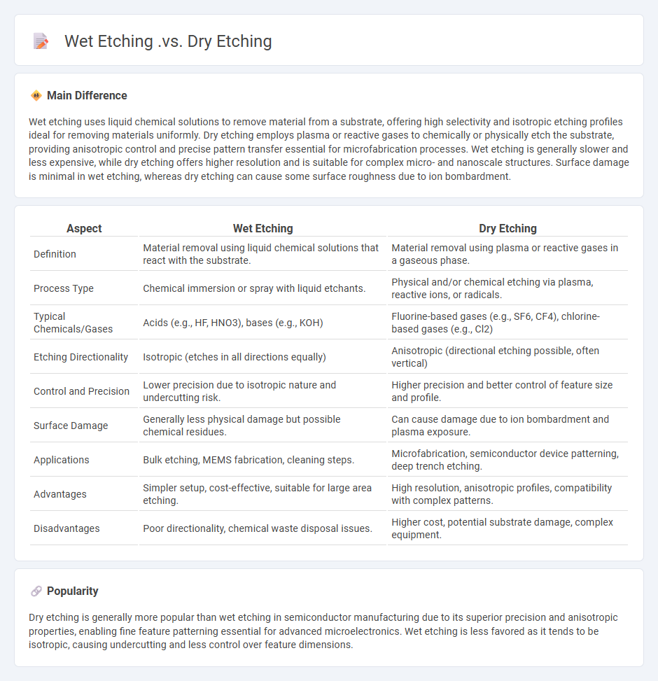
Wet etching uses liquid chemical solutions to remove material from a substrate, offering high selectivity and isotropic etching profiles ideal for removing materials uniformly. Dry etching employs plasma or reactive gases to chemically or physically etch the substrate, providing anisotropic control and precise pattern transfer essential for microfabrication processes. Wet etching is generally slower and less expensive, while dry etching offers higher resolution and is suitable for complex micro- and nanoscale structures. Surface damage is minimal in wet etching, whereas dry etching can cause some surface roughness due to ion bombardment.
Connection
Wet etching and dry etching are both fundamental semiconductor fabrication processes used to selectively remove material from a substrate to create micro- and nanoscale patterns. Wet etching utilizes liquid chemical solutions such as acids or bases, providing isotropic etching profiles, while dry etching employs plasma or ion beams for anisotropic and highly controlled material removal. These complementary techniques are often integrated within semiconductor manufacturing to achieve precise patterning and feature definition in devices like integrated circuits and MEMS.
Comparison Table
| Aspect | Wet Etching | Dry Etching |
|---|---|---|
| Definition | Material removal using liquid chemical solutions that react with the substrate. | Material removal using plasma or reactive gases in a gaseous phase. |
| Process Type | Chemical immersion or spray with liquid etchants. | Physical and/or chemical etching via plasma, reactive ions, or radicals. |
| Typical Chemicals/Gases | Acids (e.g., HF, HNO3), bases (e.g., KOH) | Fluorine-based gases (e.g., SF6, CF4), chlorine-based gases (e.g., Cl2) |
| Etching Directionality | Isotropic (etches in all directions equally) | Anisotropic (directional etching possible, often vertical) |
| Control and Precision | Lower precision due to isotropic nature and undercutting risk. | Higher precision and better control of feature size and profile. |
| Surface Damage | Generally less physical damage but possible chemical residues. | Can cause damage due to ion bombardment and plasma exposure. |
| Applications | Bulk etching, MEMS fabrication, cleaning steps. | Microfabrication, semiconductor device patterning, deep trench etching. |
| Advantages | Simpler setup, cost-effective, suitable for large area etching. | High resolution, anisotropic profiles, compatibility with complex patterns. |
| Disadvantages | Poor directionality, chemical waste disposal issues. | Higher cost, potential substrate damage, complex equipment. |
Chemical Solution
Chemical solutions in engineering involve the precise formulation of liquid mixtures composed of solvents and solutes to achieve desired reactions and material properties. These solutions are critical in processes such as corrosion inhibition, chemical cleaning, and electroplating, where specific concentration and pH control optimize performance. Engineering applications rely on standards like ASTM and ISO to ensure solution consistency, safety, and effectiveness in industrial environments. Understanding solubility, reaction kinetics, and thermodynamics enables engineers to tailor chemical solutions for enhanced durability, efficiency, and sustainability in manufacturing.
Plasma Etching
Plasma etching is a critical process in semiconductor manufacturing that uses ionized gases to remove specific material layers with high precision. This technique enables the fabrication of intricate microelectronic circuits by providing anisotropic etching profiles, essential for defining nanoscale features on silicon wafers. Common plasma gases include fluorine-, chlorine-, and oxygen-based chemistries, selected based on the target material and desired etch rate. Control over plasma density, ion energy, and chamber conditions ensures consistent etching results, improving device performance and yield in integrated circuit production.
Isotropy vs. Anisotropy
Isotropy in engineering materials refers to uniform properties, such as strength and thermal conductivity, in all directions, whereas anisotropy indicates directional dependence of these properties. Common isotropic materials include metals like aluminum and steel, exhibiting consistent mechanical behavior under stress. Composite materials and wood often display anisotropy, with varying stiffness and strength along different axes due to their internal structure. Understanding these differences is critical in design for load-bearing applications, thermal management, and failure analysis.
Material Selectivity
Material selectivity in engineering refers to the strategic choice of materials based on specific properties such as strength, durability, thermal resistance, and cost-effectiveness to optimize performance in various applications. Engineers evaluate material characteristics like tensile strength, corrosion resistance, and machinability to ensure suitability for structures, machinery, or electronic components. Advanced materials such as composites, alloys, and polymers are increasingly utilized to meet stringent operational demands and environmental conditions. The integration of material selection software and databases accelerates decision-making processes in engineering design and manufacturing.
Microfabrication Applications
Microfabrication techniques play a crucial role in engineering by enabling the precise manufacturing of microscale structures, essential for the development of microelectromechanical systems (MEMS), biomedical devices, and microfluidic chips. Common methods such as photolithography, electron beam lithography, and reactive ion etching allow engineers to achieve feature sizes down to the nanometer scale. These processes support advancements in sensors, actuators, and integrated circuits, driving innovation in telecommunications, automotive technology, and healthcare. The integration of microfabrication in engineering enhances product functionality, reduces material usage, and improves overall system performance.
Source and External Links
Wet Etching vs. Dry Etching - PCB Design & Analysis - Cadence - Wet etching uses simpler equipment and liquid chemicals offering isotropic etching with high etch rates but less precision, while dry etching uses complex plasma systems providing anisotropic, highly precise etching suitable for semiconductor patterning but with risks of surface damage and toxic by-products.
Dry Etching and Wet Etching - Thierry Corporation - Wet etching involves chemical solutions causing isotropic corrosion for cleaning and large area material removal, while dry etching uses reactive gases for anisotropic etching primarily in circuit-defining steps, requiring etch-resistant masks for protection.
What Is the Difference Between Wet and Dry Etching? - Zintilon - Wet etching features high etch rates, high selectivity, and low-cost setups but limited control and isotropic profiles; dry etching offers better process control, anisotropic etching, smaller feature sizes, but with higher cost, moderate selectivity, and potential substrate damage.
FAQs
What is etching in semiconductor fabrication?
Etching in semiconductor fabrication is a process that removes specific layers from a wafer surface using chemical or plasma methods to create patterns essential for device structures.
What is the difference between wet etching and dry etching?
Wet etching uses liquid chemical solutions to remove material, providing isotropic etching, while dry etching employs plasma or reactive gases for anisotropic, precise material removal in semiconductor fabrication.
How does wet etching work?
Wet etching works by immersing a material, typically a semiconductor or metal, in a chemical solution that selectively dissolves specific layers based on their chemical properties, enabling precise pattern transfer in microfabrication.
How does dry etching work?
Dry etching uses reactive gases or ions in a plasma state to chemically or physically remove material from a substrate during semiconductor manufacturing.
What materials can be etched with wet etching and dry etching?
Wet etching can etch silicon, silicon dioxide, silicon nitride, metals like aluminum and copper, and photoresist. Dry etching can etch silicon, silicon dioxide, silicon nitride, metals, polymers, and compound semiconductors such as GaAs and InP.
What are the advantages of wet etching versus dry etching?
Wet etching offers advantages such as higher etch rates, lower equipment costs, simpler process setup, better selectivity for certain materials, and reduced damage to the substrate compared to dry etching.
What are the disadvantages of dry etching compared to wet etching?
Dry etching disadvantages include higher equipment costs, potential for substrate damage due to ion bombardment, lower etch rates for some materials, and difficulties in achieving isotropic etching compared to wet etching.